This thread has been locked.

If you have a related question, please click the "Ask a related question" button in the top right corner. The newly created question will be automatically linked to this question.

INA827: Offset in INA823 when RG on INA827

Part Number: INA827
Other Parts Discussed in Thread: INA823, TMUX1108, INA818, TMS320F28379D

Hello everyone,
I currently have the problem that I want to record a signal with two different amplifications.
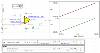
I'm using the INA823 for the low gain and the INA827 for the higher gain (was still in the cupboard).

I had problems with a too high offset in the INA823, where at 0V input voltage the output was 140mV.
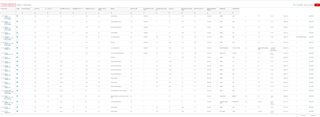
I then assembled the board piece by piece and looked at the point at which the problem occurred.
The result was that the offset goes from about 0V to 140mV as soon as the RG of the INA827 is populated (RG=9kOhm, G=13.8).

Does anyone have any idea what this could be due to?

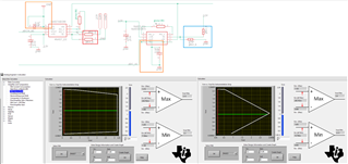
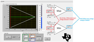
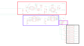
Here is a snip of the circuit:
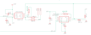

Best regards
Leon

  • I have now tested further.
    At a gain of about 6, i.e. RG=82K, and at a gain of about 7, i.e. RG=39K, the offset is not yet there. But a noise appears at both INA, which has 5-20Hz and which in the offset raises the output from 5mV to 22mV, i.e. by 440%.

  • Hey Leon, 

    What are the measured DC voltages measured at the inputs of the INA823. I see that the inverting terminal has a resistor divider from the supply but for the non-inverting terminal I am unable to tell what potential it is going to. I need to know the input common mode voltage to verify if it is operating within the linear operating range of the device. 

    Below I have created 2 scenarios demonstrating the valid common mode ranges with two different reference values. The  allowable input differential voltages are calculated accordingly. Adjusting the reference voltage adjusts the allowable linear voltage input range and output range.

    For this reason I need to know the input common mode range. The gain value will also adjust these parameters shown below.  The analog engineers calculator can be found here:

    https://www.ti.com/tool/ANALOG-ENGINEER-CALC

    Vref = 0V and Vcm = 1V:

    Vref = 1.65V and Vcm = 1V:

    Best Regards, 

    Chris Featherstone

  • Hey Chris,
    Here is the basic information about the circuit:
    INA823:
    - Inverting input is connected directly to ground via a 0 Ohm resistor (RD2_E). The RD1_E is DNP.

    - The non-inverting input is connected to several resistive sensors via a TMUX1108 demultiplexer. On one side, the sensors are also connected to 3.3V via a TMUX1108 (sensor matrix) and on the other side they are connected to ground via a Schottky diode and a 10k resistor. The sensors have about 10MOhm in the unloaded state and about 1.8kOhm under maximum load. This means that the voltage range at the IN+ input is between 3mV and 2.6V.

    - Gain: 100kOhm, i.e. a gain of 2.

    INA827:
    - inverting input voltage divider of 470 Ohm (RD5_E) and 1kOhm (RD4_E) results in a potential of 2.24V

    - non-inverting input is the same as INA823

    - Gain: we have tried open, 82kOhm, 39kOhm and 10kOhm. Between open and 39kOhm the noise of the INA823 increased and at 10kOhm there was an offset, although this only changed the RG of the INA827.

    I hope this is all the information you need. Thank you very much for your help.

  • Hey Leon, 

    If the situation is as below with ref = 0V the minimum non-inverting voltage is 1.011 V and max of 1.207 V. The minimum differential voltage is 21.429 mV and the maximum differential voltage is 414.285 mV. If I am interpreting your description correctly the min and max voltage seen at the non-inverting terminal is outside of the bounds below. It also appears the differential voltage exceeds both the min and max values calculated below meaning that the device is operating in the non-linear region and the inputs are getting pulled apart 2.19V (2.6V-414.285mV) more than the allowable linear operating range. This may be an application that would be better suited with a rail to rail op amp since it is a single ended measurement. 

    Best Regards,

    Chris Featherstone

  • Hey Chris,
    So again from my understanding of the input voltages:
    INA823:
    - Non-inverting input: 0.003-2.6V
    - Inverting input: Ground thus 0V
    - minimum differential voltage: 0.003V
    - maximum differential voltage: 2.6V

    INA827:
    - Non-inverting input: 0.003-2.6V
    - Inverting input: Ground thus 2.24V
    - minimum differential voltage: -2.237V
    - maximum differential voltage: 0.36V

    But I think you have misunderstood the problem. The INA823 works perfectly as long as the INA827 does not have a mounted RG, so it has a gain of 5. As soon as the RG is mounted, a noise comes into the output of the INA823 and with an RG of 10K at the INA827, the INA823 gets an offset that is not there before.

    For me, this means that the INA827 influences the output of the INA823 and I don't know why this can happen. In principle, I have already used the same circuit for other boards, except that I used two INA818s and two INA827s in each case. In the current project, however, I don't have a 5V supply for the INA818 and the one measuring range needs a gain between 1-2, which means that no INA827 can be used there. That's why I replaced one of them with an INA823, as I thought it would behave in the same way as the INA827.

    Do you have any idea where this influence of the INA827 on the INA823 can come from or how I can prevent it?

    Best Regards,

    Leon

  • Hey Leon, 

    I will re-read the post to try to understand the issue better. We may need to setup a Webex call. 

    INA823:
    - Non-inverting input: 0.003-2.6V
    - Inverting input: Ground thus 0V

    These conditions violate the linear operating range of the device and unexpected errors and results will occur. 

    The INA827 has a wider common mode range than that of the INA823. I will check your setup in Tina Ti simulation to better understand the issue. 

    Best Regards, 

    Chris Featherstone

  • Hey Chris,
    we can try a Webex call, but since I'm in Germany, we'll have to see what time we do it. What times are you available?

    Thanks a lot
    Leon

  • Hey Chris,
    I have removed the RG from the INA827 and the offset has disappeared. I then took calibration measurements with the sensors to check the behavior. The following are 5 series of measurements from the same sensor. The measurement results are in "digits" as raw output of the ADC.


    The tolerances may be due to the test setup, which is not optimal in the short term.
    Both output voltages of the INA823 and the INA827 are recorded in parallel. I then used the gains (INA823 now G=1; INA827 now G=5) and the potentials at the inverting inputs (INA823 In- = 0V; INA827 In- = 2.115V) to calculate and compare the voltages at the non-inverting inputs of the two amplifiers. The result was that the calculated difference is -0.00899 +- 0.00695V.
    I do not think that the problem can be due to the non-linear range of the INA823.

    Best regards
    Leon

  • Hi Leon, 

    One of the issue is that you are using our 36V high voltage IA for 3.3V near minimum low IA operation (and using single supply rail). We have plenty low voltage IAs that will work for your application. 

    https://www.ti.com/amplifier-circuit/instrumentation/products.html?keyMatch=instrumentation%20amplifier#358max=5.5%3B5.5&sort=773min;asc&

    In INA823, the Vout has the minimum output requirements. So I would recommend to try out LM7705, -0.232V inverter, and it may resolve your issues. 

    This is my suggestions, and I have not read your replies. 

    Best,

    Raymond

  • Hi Leon,

    Here is the INA823 simulation. The 140mV Vos is likely resulted from the linear Vout operating range, which is from (-Vs) + 150mV to (+Vs) -1. The specification is assumed symmetrical dual supplies. Since your circuit is configured as -Vs = GND, the Vout_min = 150mV and Vout_max = 3.3V - 0.15 = ~3.15V range. Unfortunately, the Spice model did not demonstrate this behavior for some unknown reasons, and we are unable to see the simulated behaviors. However, you will observe the behavior from the physical INA823 operation with Vs = 3.3Vdc as the single supply rail.  

    As I previously indicated, INA823 is tailored for higher voltage operation, though it may operate down to 3.3Vdc (2.7Vdc minimum for the single supply rail). When the application is operating in the low voltage range in a single supply rail, there are certain limitations, which you are observed in your configuration.    

    INA823 3p3V Operation 05022024.TSC

    If you have other questions, please let me know. 

    Best,

    Raymond

  • Hey Raymond,
    Thanks for your effort. It all sounds logical so far.

    I have been using the INA827 (single supply 3.3V) and the INA818 (single supply 5V) for a long time and have never had such problems.

    What irritates me is that the problems only occur when the amplifying resistor RG is fitted to the second IA (INA827) which amplifies the same signal. Before that, the INA823 shows the known behavior without the offset. For me, this means that the INA827 has a feedback effect on the INA823 either via the Vin+ or the ground, which I cannot understand. In other PCBs I always had two IA on one signal but always the same (either INA818 or INA827). And I have never had this phenomenon before.

    best regards

    Leon

  • Hi Leon, 

    Could you provide me the actual values used in the configuration in the marked orange, red and torques blocks? What are your input Vcm and the differential input voltage ranges? I will take a look. 

    I assumed that both IAs are sharing the same input with the identical Vcm mode applied to the input. Maybe input or output impedance or feedback have interference issues that result the strange behaviors.  Are 0.1uF capacitors always shorted to GND at Vref; and the Vref voltages are terminated to GND at Vref pin at each IA? What is the input differential frequency range for IAs?

    From the IA calculator, the input and Vout ranges of two IAs seem to be operating in the similar range. 

    Best,

    Raymond

  • Hey Raymond, 

    Below you will find the information you wanted:

    Both Non-inverting input: 0.003-2.6V


    INA827:

    - inverting input voltage divider of 470 Ohm (RD5_E) and 1kOhm (RD4_E) results in a potential of 2.24V
    - minimum differential voltage: -2.237V
    - maximum differential voltage: 0.36V

    INA823:
    - Inverting input is connected directly to ground via a 0 Ohm resistor (RD2_E). The RD1_E is DNP.

    - minimum differential voltage: 0.003V
    - maximum differential voltage: 2.6V

    CD1 & CD2 0.1 mircoF

    Unfortunately, I don't know how to calculate the Vcm from this.

    The sensors are currently measured at a frequency of 12.5 kHz. I have already reduced this with the PCBs with two INA827 and INA818 I have measured the sensors with a frequency of about 90kHz.
    I hope I haven't forgotten anything and that you can make use of the information.

    Thank you and best regards
    Leon

  • Hi Leon, 

    Thanks for the IA's parameters. I am trying to figure out what the system hardware configuration is. Sorry, certain parameters are still missing. 

    Both Non-inverting input: 0.003-2.6V

    Based on the information, one of the input signal (Vin+) swings between 3mV to 2.6V @12.5kHz. The mid point of the AC input signal is  (3mV+2.6V)/2 =1.3015V. 

    So the AC input signal swings above and below 1.3015V with amplitude of ±1.2985Vpk at 12.5kHz. 

    INA827:
    - inverting input voltage divider of 470 Ohm (RD5_E) and 1kOhm (RD4_E) results in a potential of 2.24V
    - minimum differential voltage: -2.237V
    - maximum differential voltage: 0.36V

    The (Vin-) terminal in above INA827 has a fixed DC potential at 2.24 (Vin+ = 2.2449Vdc). The (Vin+) - (Vin-) delta is the differential input voltage. 

    Min. differential input AC signal @12.5kHz: (Vin+) - (Vin-) = 2.24V - (-2.237V)  = 4.84V, which is > 3.3V or not possible. Other possible range is 2.24V - 2.237V = -3mVpk

    Max. differential input AC signal@12.5kHz: (Vin+) - (Vin-) = 2.24 - 0.36V = 1.88Vpk

    The common mode voltage, Vcm, should be [(Vin+) + (Vin-)]/2, which it should be close to a fixed DC. AC input signals are riding on the Vcm mode in the input of the instrumentation amplifier.  

    Since the differential input signals swing from -0.36V to 2.237V in large amplitude in INA827 (in your 3.3V single supply rail), there may be a piece of information that is missing from the circuit's parameters. Enclosed is the link of the IA calculator for your reference. 

    https://www.ti.com/tool/ANALOG-ENGINEER-CALC

    . The result was that the calculated difference is -0.00899 +- 0.00695V.

    The above statement indicates the differential input may be from -15.94mV to -2.04mV, which implies that input signals are in mV range, not from mV to V range. And the IA's Gain is configured more than 1 V/V. 

    Could you provide me your working INA818 IA configuration? I may be able to provide information how it may work in the previous setup. 

    If you have other questions, please let me know. 

    Best,

    Raymond 

  • Hey Raymond,
    thank you very much for your effort, I really appreciate it.

    Here is a complete explanation/description of our circuit.

    We measure with a matrix of FSR400 pressure sensors. The matrix is divided into columns and rows and is read out via two TMUX1108 multiplexers/demultiplexers (blue box). The MUX_V is operated as a 1 to 8 multiplexer and ensures that only one column of the matrix is connected to the power supply at a time. The columns of the sensor matrix are connected to the "ColumnX" connections. The MUX_A is used as an 8 to 1 demultiplexer and ensures that only one row at a time is connected to the IA. The sensors are connected to the individual rows via BAT54C diodes (black box) and these are then connected to the MUX_A. The individual lines are also each connected to GND via a 10k resistor so that the change in resistance of the sensors can be measured.
    The output of the MUX_A is connected to the two IA (red box). The circuit already described is located there and both IN+ of the IAs are connected to the output of the MUX_A.
    The control of the multiplexers via PWM signals and the ADC of the IAs outputs is realised with the MCU TMS320F28379D.
    The idea behind the two IAs is that we want to divide the same signal into two measuring ranges in order to obtain a good resolution for both low and high measured values. The IN inputs are then used to cut off one range of the signal and amplify the rest.

    The previously stated 12.5kHz and 90kHz is the frequency at which the multiplexers switch between the sensors. The signal from each sensor is relatively static over a measurement as such with no major changes.

    The measurement signal at the non-inverting inputs can be between 3mV and 2.6V as the sensors can be between a few MOhm and about 1.8kOhm.

    You probably misunderstood my statement about the calculated differences. Chris meant that we are probably in the non-linear range of the INA823. I then carried out a series of measurements and compared the output voltages recorded in parallel. Or I calculated the voltage at IN+ from the output voltages for both IAs and compared them. This resulted in the said differences of -0.00899 +- 0.00695V, which means that I do not assume that we are working in the non-linear range.

    Here again are the configurations we used:
    1. INA823+INA827:
    RD1_E = DNP, RD2_E = 0 Ohm, RD4_E = 1 kOhm, RD5_E = 560 Ohm, R_V_1 = DNP, R_V_2 = DNP
    -> no problems

    2. INA823+INA827:
    RD1_E = DNP, RD2_E = 0 Ohm, RD4_E = 1 kOhm, RD5_E = 560 Ohm, R_V_1 = DNP, R_V_2 = 10 kOhm
    -> Offset in the output of the INA823

    3. INA827+INA827:
    RD1_E = 17.4 kOhm, RD2_E = 10 kOhm, RD4_E = 34 kOhm, RD5_E = 10 kOhm, R_V_1 = DNP, R_V_2 = 13.3 kOhm
    -> no problems

    4. INA818+INA818:
    RD1_E = 1 kOhm, RD2_E = 1.05 kOhm, RD4_E = 1 kOhm, RD5_E = 1.4 kOhm, R_V_1 = 12.5 kOhm, R_V_2 = 5 kOhm
    -> no problems

    The different Vin- and gain values are due to the fact that we measured different things.

    We do not have AC signals but clocked DC signals. I think now that the circuit has been explained in more detail, it may be easier for you to understand/find the problem.

    Best Regards,

    Leon

  • Hi Leon, 

    Thanks for the additional information. 

    we can try a Webex call, but since I'm in Germany, we'll have to see what time we do it. What times are you available?

    This is good option. I will contact you next week. 

    I am going to close this query, since we have established contacts via E2E private messaging system.

    Best,

    Raymond