ADS8568: Settling within 1/2 LSB

Part Number: ADS8568
Other Parts Discussed in Thread: OPA2156, OPA2277, OPA211

Tool/software:

Hi All,

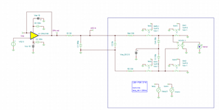
I'm trying to design the input stage driver for the ADS8568, from the datasheet here is the input stage

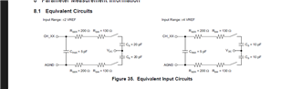
Using the analog engineers calculator I got the following values:

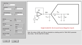
I selected the OPA2156 as the driver and have a 5V fixed input for now (first trying to get the input settling correct before any signal conditioning circuitry is added).

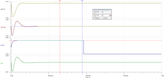
Running the OPA2156 in open loop I have the output as:

The acquisition time is set to 280ns and the sampling rate is 400k.

For the life of me using the recommended values I cant get it to settle within 1/2 LSB which is ((10V/65535)/2) =  ~76uV

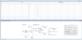
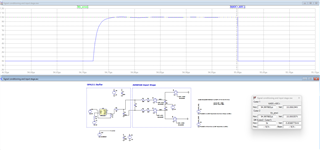
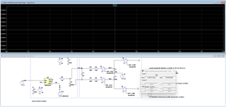
Here is one of the simulations I ran:

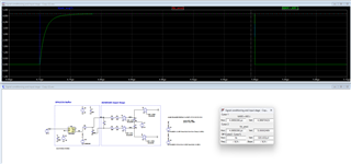
The GBW of the amplifier is within spec and I'm not sure why the amplitude does not settle sufficiently.

Any help will be appreciated.

Thanks in advance

  • Hello Pieter,

    This is interesting, ideally with the filter you selected it should be settling within ~230ns. All of the components chosen should work well with the device.

    I tried this simulation in Tina TI and I got a settling point, it did however seem to need a bit longer than the minimum acquisition time 

    Is there anyway you could do a regressive settling calculation instead or place a measurement point on ADC in when the full circuit is connected?

    Best regards, 

    Yolanda

  • Hello Yolanda,

    I did extend the acquisition time and it does settle in ltspice after ~382 ns.

    "Is there anyway you could do a regressive settling calculation instead or place a measurement point on ADC in when the full circuit is connected?"

    I am not too sure what you are requesting but with a bit more information I will be more than happy to do some legwork and return with info. From the latter point it sounds like you would like to measure the hardware. At this point in time I am busy designing and doing PCB layout so everything is running in simulation.

    Please note that if there is a different buffer more suited to the ADS8568 I will happily consider it.

    Looking forward to your inputs. Thank you

  • Hello Pieter, 

    I apologize for the confusion with my wording. I was trying to ask if a probe could be placed at the OPA output and used as reference in the settling measurement, in case the output of the opamp was changing. It shouldn't have though, please disregard.  This would have all still be in simulation, but thank you for offering the leg work with the info.  

    The OPA2277 is what is recommended on the datasheet but in this case where settling is important I would suggest looking into the OPA828 or the OPA211

    Best regards, 

    Yolanda

  • Hello Yolanda,

    Thank you, I have implemented the OPA211 in my design and settling looks great.

    The device settles well within 1/2 LSB, I have also increased the input voltage to 10V as a design change.

    1) my next question would be are the equations used to determine the values of the charge bucket filter documented somewhere? I have watched the TI precision labs video but they only refer to the analog engineers calculator. I would like to be able to derive the circuit values from first principles.

    Now that I can confirm that the circuit can be driven within spec I would like to do some signal conditioning, this is something I have looked at yet I havent found a solution that works well. Essentially the input signal will be unipolar ( 0 ->10V) and I would like to drive the full scale range of the ADC (-10V ->10V).

    I have looked at using the level shifter with gain circuit recommended on a few TI forum posts but this seems to negatively affect the settling

    I have also tried to use a INA with a reference offset but sadly it seems the output is limited to far less than the positive rail in my simulations.

    Do you possibly have any recommendations for a circuit? I do not mind keeping the opa211 as only the buffer/driver and having the signal conditioning done by another circuit prior to it.

    Thank you for all the help

  • Hello Pieter,

    I am glad the OPA211 is working well at least for settling. It does seem like it might have gotten a bit unstable with the added gain and change in filter load. 

    Maybe I can be more helpful if I could have some insight on the type of system that this circuit is going in or what kind of inputs the ADC is expected to see, would you mind sharing some more about that?

    If you'd like to understand and personally do more of the calculations we do have some documents explaining different device functionalities, circuits, and how to derive component values.  I think this one might be particularly interesting in this situation since it is using the same device with somewhat of a similar supply and input.  

    More like these can actually be found within the same Analog Engineer's Calculator. There is a tab named "Cookbook Search" under "Data Converters" where there is a searchable list of design documents related to ADCs that can be helpful and have ways to calculate different aspects of an ADC as well as different types of example reference circuits (Also and extended version is accessible here: https://www.ti.com/design-development/analog-circuits.html

    Best regards, 

    Yolanda

  • Hi Yolanda,

    Thank you for the detailed response.

    May I send you more details via a personal message regarding the application?

    I will review the rest of the documents provided and might ask a question or two regarding the calculations. 


    Thank you for all the help thus far