LMH6629: Strange SNR-calculation in AppNote SNOA942 TIA: Choosing the Best Amplifier for the Job

Part Number: LMH6629
Other Parts Discussed in Thread: OPA855

Tool/software:

Hi all

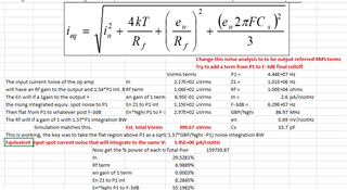
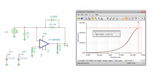
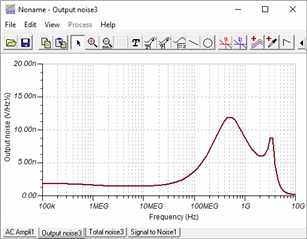
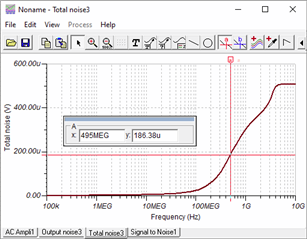
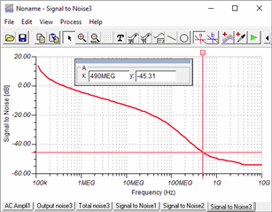
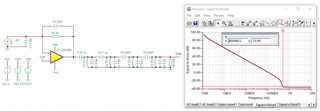
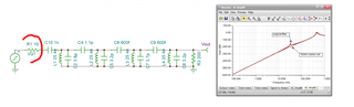
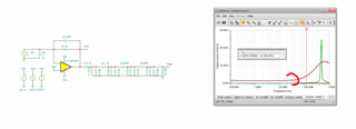
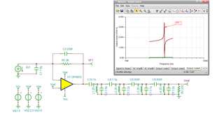
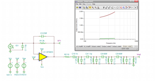
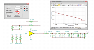
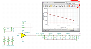
Can someone help me understand the SNR calculation in Table 1 of SNOA942?

The footnote reads: (5) SNR computed as ratio of minimum signal (10nA) to input referred spot noise ini [= 20 * log(10nA / ini) ]

As i see it, ini is a current noise density [pA/RtHz] whereas the 10nA is the minimal photodiode current.

How can you calculate the SNR as a ratio between a current and a current density?

  • Hi Lukas,

    I was able to look through the app note, and it does get a little confusing. The value Ini that is used to get SNR is the input referred spot noise of all the sources added together calculated using equation 2. It is not the current noise density value shown as In in the table. Hope this makes more sense.

    Best Regards,

    Ignacio

  • Hi Ignacio,

    Thanks for your answer, but i am still confused. Let's take the example of LMH6629:

    First, there is the OpAmps input-referred current noise in=2.6 pA/RtHz. Then there are the noise terms:
    Noise Current Term = 2.6 pA/RtHz (equals in)
    Noise Voltage Term = 0.07 pA/RtHz
    Thermal Noise Term = 1.3 pA/RtHz
    Input Capacitance Term = 2 pA/RtHz
    input referred spot noise ini = sqrt(sum of squared noise terms) = 3.5 pA/RtHz

    Then, SNR is calculated as: SNR = 20log(10nA/3.5pA/RtHz) = 69 dB
    This neglects the Bandwidth of 80MHz and is only valid for a 1Hz BW.

    Imho it should be: Ini = ini*sqrt(BW) = 3.5 pA/RtHz * sqrt(80MHz) = 31 nA
    This results in a not so great SNR = 20log(10nA/31nA) = -10 dB

    Do you agree?

  • Hi Lukas, 

    I had actually not reviewed Hooman's app note here before - he made a few mistatements adapting this from some of my material. And I have added a few things to this over the years, Here is a snip from the noise part of my current TIA spreadsheet. Let me describe each term, this is set up for that LH6629 row in table 1 where, 

    with 10kohm Rf and 10pF source diode (and you have to add the input Ccm + Cdiff) add 5.7pF to that so you are designing for a 15.7pF source C. The Cf calculation in Figure 2 is wrong - to get that F-3dB result, that 2 in the denominator of the Cf equation should be a 4. That will set the feedback pole at 0.707* Fo and then loop back to give you a closed loop F-3dB at Fo with a butterworth response. 

    Anyway, this calculates to require a Cf = 0.36pf and as Hooman mentions that last term in the noise equation he shows (from an early article I did) is the peaking noise gain inside this design. 

    The difficulty is that each noise term as a different freqency respone to the output - the approach I have gone to is to get an Eo_ RMS term to the output including that freqeuncy response. The equations set up below are not bandlimiting by any postfilter (which that earlier equation was assuming) and just let it self limit by the higher F noise gain (whcih is quite high in this example) and the GBP intersection to give a single pole rolloff - this is quite complicated, but here goes, 

    This equation was assuming F was being post bandlimited at something less than the feedback pole itself, so it is an integral along that rising noise gain curve stopped at some F below the feedback pole. I was always recommending that to avoid that dominant integrated noise term from the feedback pole to the self limited by GBP/NGhigh. This equation is input referred, but the calculation below it is developing output Vo terms in some BW then RMSing those - the dominant term in that table at the bottom is always the high frequency noise gain times the input voltage noise out to the self limited single pole bandwidth, it has been awhile since I was working on this, but I made the comment it matches TINA sim results. The point here (without getting into all the detail), that F in the equation is only valid if that is a sharp postfilter cutoff below the feedback pole - which is a pretty good idea. 

  • And continuing that example in Table 1, here is that piece of the TIA design effort, where it predicts a (with Q=0.707 butterworth) 62Mhz F-3dB, Tina gives 

    TINA gives 56MHz, so pretty close, this stuff is somewhat approx. since what I have done is drop the Cf (which we don't know initially) out of the noise gain zero frequency which the algrebra shows it is there, 

    Then, here is the output spot noise, 

    That output spot noise peaking is not as dramatic as I was expecting, probably the input current noise and Rf noise are both rolling off at P1, the feedback pole as the voltage noise peaking is also coming up, 

    My spreadsheet was predicting 400uVrms at output, the sim out to 500MHz shows 500uVrms, so a little off, but the real point here is you need some form of noise bandlimiting (even a simple RC) at the amplifier output, 

    Now TINA lets you do a SNR but you have to define the input RMS current level for that calculation. I will put in 10nA as the RMS input current signal to consider. yes this is really bad with that low of an input signal and this wide a bandwidth integrating all that noise, 

    and it gets worse, you also have to consider any dark current noise as an added input noise current - never in these sims that current source input is noiseless, you have to add it manually. And, most recently I have been sensititzed to the fact that the detector signal current is also a shot current noise source, I had one guy tell me that was always actually dominant. A lot of these channels bandlimite a lot and average for these reasons. 

    LMH6629 sim for transimpedance 10pF source.TSC

  • Hi Michael,

    Thank you for explaining, much appreciated! I'm new to TIA Design and trying to get things sorted out. My actual design aims at high bandwith and high dynamic range. I selected OPA855 and calculated Cf using the TIA_Calc spreadsheet I found here: https://www.ti.com/document-viewer/lit/html/SSZTAY1

    Calculated:
    f-3dB = 495 MHz
    Total output integrated = 266 uV

    Simulated:
    f-3dB = 490 MHz
    Total output integrated = 186 uV  - a little off as well
    SNR with 1uA RMS input current: -45 dB

    I tried a 5th order bandpass filter, but SNR is still -33 dB with a 1 uA input. But my signal around 450 MHz is actually narrowband, so i guess i have to tackle SNR differently...

    Can you give me a hint about stability? I follow layout recommendations of the OPA855 datasheet, what else should i keep in mind?

  • can you insert your TINA file

  • Here it is. I got the OPA855 Reference design from here: https://www.ti.com/lit/tsc/sbomap7

    TIA OPA855 sbomap7c.TSC

  • Thanks, here is the filter with and without a series 10ohm into it. don't normally see these filters without some driving point impedance, and the original has a resonance around 30Mhz, 

    And the the original cricuit spot noise at the output pin and the filter output, that little blip at 30Mhz needs zooming in, 

    Not sure this is a good thing, 

    Try putting in the series 10ohm, that looks a little better, likely the 0ohm output one has some interaction with th eopen loop output impedance

    And then as we set up for an SNR test, it going to integrate the noise through the whole bandwidth but I think we compare that to the signal level at the noise measurement point, not the input signal, here that is with 2mVrms output signal (could be wrong here, been awhile since I was doing this)

    and now we see about 31dB SNR at the final filter output, 

  • 31 dB - now I like that figure much better! We have to compare output noise to output signal - makes sense.

    I added the 10 ohms in series. Good point.

    Thanks a lot for your support. I'm gonna build the design and find out what the simulation is worth ;)
    Many things i didn't consider in simulation, e.g. parasitic inductance of APD in TO-can ... but I'll give it a go.