INA202: Incorrect overcurrent trip at high temperatures

Part Number: INA202
Other Parts Discussed in Thread: INA310B

Tool/software:

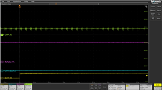
Recently, we have a high number of digital output modules failing during a functional test at high temperatures.

The cause was determined to be a faulty function of the INA202 at high temperature (INA202AIDGKT).

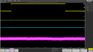
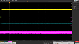
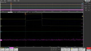
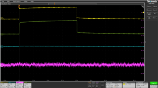
Output is tripped out when switching the output (to zero load) above 70°C approx.

(There is a high side digital out with overcurrent protection with INA202.

During switch-on, the overcurrent protection is activated even though the load and external voltage is not connected).

We are trying to collect more data about this phenomenon.

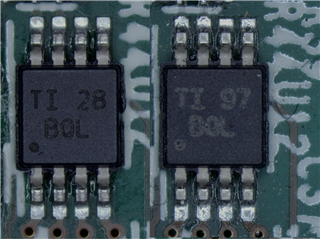
During the optical inspection of the modules, we discovered a different package marking technology on the devices soldered on new modules.

In the first problematic batch of modules, the devices has number "28" on the case. Now we also have the problematic devices with number "34".

On older batches of modules, the number on the device case is "97", and there have never been any problems with them (or very rarely).

Here is the marking comparison between "97" and "28". Marking technology of "34" (I have no photo yet) is similar to "28".

Marking comparsion

We need help in determining the root cause of the problem.

  • The guaranteed datasheet limits have not changed. Below the minimum recommended supply voltage of 2.7 V, correct operation is not guaranteed.

    Section 9.1 of the datasheet says:

    Figure 38 shows the typical output voltages for high and low-side configurations with the given ramp supply voltage. These fluctuations on the output during power-up may require a controller to incorporate a blanking time to disregard the artifacts.

  • The problem is probably not related to the power supply. Device is powered by 12V source.

  • What exactly do you mean with "during switch-on"? What voltages at what pins change? Please show the schematic and an oscilloscope trace.

  • INA202 is used in NFET high-side switch with overcurrent protection.

    "During switch-on" means: NFET high-side switch is switched-on (but without external power and external load connected => no current).

    I attached a part of the schematic (slightly modified for clarity without knowing the context of other connected circuits).

  • Hello Jiri,

    I cannot see an issue yet.  Are you able to measure the output pin (2) or the CMPin pin (3) to verify the inputs?  Also R46 and R44 are high and IB into the device could cause offsets but not big enough for your issue.  I would still verify that the input voltages are as expected and close to GND_DRV.

    I see the markings are different did you get the devices through TI.  Can you track the lot code from your order?

    I can see that you are only using it as a comparator.  If you were using the analog input I would recommend you transition to the INA310B.  You may want to look into transitioning to the INA310B either way after you determine the root cause of this issue.

    Regards,

    Javier

  • I made some measurements yesterday. I'll continue with a better oscilloscope later today.

    During the measurement, the output is switched periodically every 250ms (ON - 250ms - OFF - 250ms ....).

    The channel assignment is as follows:

    C1 = pin 5, OUT_EN

    C2 = pin 6, OUT_BLOCK

    C3 = pin 2, OUT

    The first screenshot shows the correct function for reference

    The second screenshot shows a faulty function when the module is heated up by hot air (switch-off after 40us is reaction of system based on FAULT signal).

    See that the OUT on pin 2 is still near zero (approx. 20mV).

    The third screenshot shows a detail of the activation of the OUT_BLOCK signal

  • About marking, lot code and device ordering - I asked our manufacturing department for information.

    What I can tell now is that last few devices for testing was ordered from MOUSER (marking 34).

  • Hello Jiri,

    I am wondering if the devices is going into the issue described in the datasheet section 7.4.2.4 although I don't expect it to go as high as you are seeing.  Did you double check the input voltages to see what they are moving to during this switching?  Does the transient at hot cause something at the input side to do something unexpected.  

    Regards,

    Javier

  • Hello Javier,

    I rebuild measurement setup with better oscilloscope. Look at the following pictures.

    C1 = pin 5, OUT_EN ; C2 = pin 2, OUT ; C3 = Vsense, measured on C39 by differential probe ; C4 = pin 6, OUT_BLOCK

    The first screenshot shows the correct function for reference

    The second and third screenshot shows a faulty function when the module is heated up by hot air (same time base as previous screenshot and zoom to switch-on area). See that the Vsense and OUT on are still near zero.


    The third screenshot shows a detail of the faulty function with 10us/div timebase.

    I definitely don't see a reason to activate the comparator based on the output of the amplifier.

    Paragraph 7.4.2.4 (Low VSENSE Case 2) which you mentioned...

    ...maybe some pieces of device have VOUT = 2V under conditions VCM = 0V, VSENSE = 0V but:

    • it does not apply to this piece regardless of temperature
    • the  VOUT = 2V is not enough to activate the comparator anyway

    Now I will change the measurement setup for measuring comparator and supply pins. 

  • After change measurement setup, I took this screenshots.

    Normal operation


    and faulty function when the module is heated up by hot air

    faulty function ones more in better detail

    Result:

    • no power drop on VS
    • no peak reaching 600mV on CMPIN
  • Hello Jiri,

    I ordered some devices and will see if I get the same issue.  Do you know what the failure rate is?  Is it only from those lots (markings) that you see the issues?  Can you replace that device with the  INA310B?

    Regards,

    Javier

  • Hello Javier, sorry for the late reply, I was on vacation.

    About failure rate - I asked our production department for a response. But it seems to me that there were no problems with the devices marked 97.

    Replace INA202 to INA310B on the faulty module is not a problem. I ordered samples for testing.

  • Hello Jiri,

    I ordered only 5 of each and will take a look at them later this week.  Depending on the failure rate I may not see the same issue.

  • Hello Javier,

    do you have any new knowledge about the problem?

  • Hello Jiri,

    I tested 10 devices and I did not see the issue you are seeing.  Did you find the failure rate?  

    Regards,

    Javier

  • Hello Javier, 

    were your tests performed at high temperature (>80°C)?

    About failure rate - is a bit difficult to find out any exact data retrospectively. But I found something...

    For understanding - our modules with INA202 (4 pcs in each) are produced by our manufacturing partner and he performs basic functional testing. Second part of testing is performed by our manufacturing department on completed unit with module mounted inside. These tests include burn-in test with ambient temperature 70°C. So, INA202 will fail during this burn-in test.

    From 2022, when production began, 182 modules (~728pcs of INA202) have been delivered by the manufacturer. The manufacturer says that some pieces were defective at room temperature and were repaired by replacing the INA202 chip. But it is not clear how many pieces were involved.

    During the burn-in tests, 33 units were identified as defective (>24%). As each module contains 4pcs of INA202, this represents something between 6-24% of defective INA202 (there are modules with more than one defective INA202).

    Unfortunately, the marking of circuits was not monitored in the past. Now, we have registered the following numbers of defective circuits (but we don't know how many pieces of what lot was used) :

    INA202 marking defective pcs comment
    TI 97 BQL 8 probably used on older production with low failure rate
    TI 23 BQL 14
    TI 19 BQL 1
    TI 28 BQL 3
    TI 34 BQL >2 only 10pcs buy 7/2024 from MOUSER for testing

    The manufacturer promised to supply data scanned from the reel in preparation for production - I will share them with you as soon as I receive them.

    At the same time I asked about the source of the circuits - there was buy from Farnell, Digi-Key, TME a directly from Texas Instruments.

  • Jiri,

    I think I will have time tomorrow to verify the 10 parts I have and vary the temperature above 80C.

    Regards,

    Javier

  • Hello Jiri,

    I was able to reproduce.  So I investigated and this is know issue and explained in the datasheet.

    Regards,

    Javier

  • Hello Javier,

    thank you for your research. I tried the workaround this morning (LPF 1nF/420R on RESET) and everything seems fine.

    I made the workaround on one output, while on the other I replaced the INA202 with an INA310B circuit.

    Now I will send the whole unit to our production department to do full long-term tests in the climate chamber.

    To fully clarify the issue:

    • LPF on RESET is only required for INA202
    • INA310B does not have similar unwanted behavior

    are these statements true?

  • Hello Jiri,

    • LPF on RESET is only required for INA202
    • INA310B does not have similar unwanted behavior

    Both statements are true.  I would recommend moving to the INA310 if possible as it is more accurate and I believe it cost less.  There are some other difference like VCM range.

    Regards,

    Javier