This thread has been locked.

If you have a related question, please click the "Ask a related question" button in the top right corner. The newly created question will be automatically linked to this question.

INA3221: Designing with INA3221

Part Number: INA3221
Other Parts Discussed in Thread: SN74LV4052A, TCA9546A, INA4230, INA4235

Tool/software:

I am working with adding INA3221 in my schematic. I am wondering about the address pin. There is only one address pin Ao. The pin Ao can be attached to GND, VS, SDA, or SCL. Does it means only four devices INA3221 can be attached to I2C bus ?

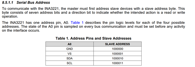
The slave addresses (7 bits) mentioned in Table 1 in the datasheet has only four different addresses which corresponds to four Ao connection options. 

Question: How can we add six INA3221 to I2C ?  

  • Another question is that possible to connect VPU (16) to VS (4) ? Can we have VS 3.3 V or it has to be 5.0 V ? 

  • To prevent address conflicts, use an I²C switch/multiplexer like the TCA9546A. If you have additional GPIO pins available, you can also use a plain switch like the SN74LV4052A.

    The VPU allows to use a PV output voltage higher than VS. But this is not required, you can have VPU = VS.

  • Thanks for addressing the issue.  

    Regarding the value of shunt resistor. I did following calculation. 

    According to datasheet, the maximum voltage across shunt resistor is +/- 163 mV. 

    I have 3.6 A max running through the power cables. The supply voltage at the load is 3.3 V. 

    I found 39 mOhm through hole resistor having power rating 3 W tolerance +/- 5%. I also found SMD with tolerance 1%. 

    The voltage across shunt resistor will be

    V = I x R 

    V = 3.6 x 39/1000

    V = 140 mV

    The power dissipation across shunt resistor will be 

    P = V x I 

    P = 140/1000 * 3.6

    P = 0.5 Watt 

    What will be the resolution of the current measurement ? 

    Considering 2 bit noise in 13 bit ADC. 

    3.6 A / 2048 = 1.75 mA 

    Is my calculation make sense for 11 bit ADC ? 

  • Hello John,

    Yes, the INA3221 can only have 4 devices on one I2C bus, but as Clemens mentioned there are some ways around that. In addition, you may be interested in our newer 4 channel devices, the INA4235 and INA4230. These have 2 address pins to support up to 16 devices on one I2C bus. 

    As for your question on accuracy, below is a link to an error tool that can help you determine if your setup is working with the INA3221. You are using 140mV out of 163mV range, so that is using most of the range, which is good. The LSB of the shunt voltage is 40µV, which converted to current would be I = V/R -> 40µ/39m ≈ 1.026 mA step size. However, as you noted, there will be noisy bits at the bottom. The amount of noise depends on your conversion time and averaging settings. 

    https://www.ti.com/tool/download/CS-AMPLIFIER-ERROR-TOOL

    The newer devices are not in this tool yet, but they do have an ENOB table (Table 8-2) in the datasheet that can help you determine the noise free resolution based on your settings. Unfortunately, the INA3221 does not have this data table. 

    Regards,

    Mitch

  • Thank you very much for your reply. I will have a look at the new devices you mentioned. 

    Regarding estimating measuring error in case of INA3221.

    I understand there will be followings to consider.  

    * ADC_offset (and drift)

    * ADC_gain (and drift)

    * ADC_noise

    * ADC_nonlinearity (INL)

    With 0.39 mOhm the current measurement size will be 

    I = V/R -> 40µ/39m ≈ 1.026 mA per bit

    We can chose bit longer conversion time to average over 256 samples.

    Is that reasonable to consider the last two bits as noise ? 

    With 11 MSB, the step size would be 4.140 mA which is fine by us. 

    According to datasheet the operating Junction Temperature is 125 degC. 

    Section 7.1 describe all the thermal resistances in the unit of degC/Watt. 

    How can calculate power dissipation. 

    I am using two channels. The power supply at the load will be 3.3 V. INA3221 power supply is 5 V. The current through each shunt resistor 0.39 mOhm is 3.6 A. How can I calculate the power dissipation through INA3221 ? I will then calculate Junction Temperature using the thermal resistances given in Section 7.1.  


  • Hello John,

    Is that reasonable to consider the last two bits as noise ? 

    It's hard to say for sure since we don't have an ENOB table for this device, however I would think that sounds reasonable. It may even be better than that. Here are a couple examples from the datasheet on how conversion time and averaging can affect noise levels:

    How can I calculate the power dissipation through INA3221 ?

    When looking at power through the INA3221, you don't need to consider the shunt sizes or the current over the shunts, you just need to look at the power going into each pin. For this you would add up the power from each source:

    Supply power: Iq * Vs

    Input pin power (for 2 pins): Ib*VCM*2

    Vbus measurement power: (VCM/Vbus_Impedance)*VCM

    Note the vbus pin impedance is spec'd in the input bias current for the IN- pin row. Also technically the input measurement and vbus measurement don't happen together, so you can average the power together based on the ratio of your conversion time settings.

    Regards,

    Mitch

  • 1- Considering the Quiescent equal to 400 uA, we can calculate the Quiescent power. 

    Supply Quiescent power: IQ x Vs = 400 u x 5 V =  2 mW

    2- Considering the input bias (IN+ and IN-) current equal to 10 uA and common mode voltage 70 mV (note that the differential voltage across shunt will be 140 mV). 

    Input pin power (for 2 pins): 2 x IB x VCM =  2 x 10 u x 70 m = 1.4 uW

    3- The last point Vbus power is not clear to me.

    Can I consider Vbus impedance as 0.39 mOhm which is the value of shunt resistor and common mode voltage equal to 70 mV ? Please comment on the common mode voltage which is found as 70 mV. 

    Vbus measurement power: (VCM/Vbus_Impedance)*VCM =  0.5 W 

    The total power will be the sum of all three contributions which is almost equal to 0.5 W. 

    According to section 7.4 Thermal Information. The Junction-to-ambient thermal resistance is 36.5 degC/W

    The junction temperature (TA) will be equal to ambient temperature (consider 40 degC) + 0.5 W x 36.5 degC/W = 58.25 degC. 


  • Hello John,

    The Vbus Impedance is 670kΩ, so if your VCM = 70mV, then (70m/670k)*70m=7.3nW, so it will be much less power.

    Also, you wouldn't just add all 3 together because vshunt and vbus aren't measured at the same time. If your conversion times for the two are equal, then you could average the two powers together, then add the power from Iq. 

    Regards,

    Mitch

  • Hello again,

    I am wondering how can I find from datasheet that the Vbus Impedance is 670kΩ ?  

    In the datasheet I found the following in 7.5 Electrical Characteristic

    IN– Input bias current at IN–    10 || 670   μA || kΩ 

    But where it says that "670kΩ" is Vbus Impedance ? 

  • I have a doubt on VCM = 70 mV. 

    The Bus voltage is 3.3 V. The value of shunt resistor is 39 mOhm. The voltage drop across shunt resistor is 140 mV which is fine for INA3221 as it can accept up to 163 mV. 

    The VCM is defined by (V1 + V2) / 2. This will be (3.3 V + 3.3 V + 140 mV ) / 2 = 3.3 V + 70 mV ? Is that right ? 

  • Hello John,

    I am wondering how can I find from datasheet that the Vbus Impedance is 670kΩ ?  

    Yes, you found the right spot. It's spec'd a little different in this datasheet than we usually spec it, but that is the location. The VBUS is measured from the IN- pin, and so that is why it is spec'd as input bias current for the IN- pin only (as a resistance, since the current depends on VBUS). Our newer datasheets are much more clear about this.

    I have a doubt on VCM = 70 mV. 

    Ah, yes, from the info you just gave, 70mV is not your VCM. Your equation is almost right, you would have a 140mV drop, not addition, so the equation would be (3.3 V + 3.3 V - 140 mV ) / 2 = 3.3 V - 70 mV. 

    Regards,

    Mitch