This thread has been locked.

If you have a related question, please click the "Ask a related question" button in the top right corner. The newly created question will be automatically linked to this question.

OPA2992: Charge Amplifier PCB Design has consistent <10 Meg Ohm Leakage path

Part Number: OPA2992
Other Parts Discussed in Thread: OPA928

Tool/software:

I designed a charge amplifier PCB with OPA2992 for the purposes of measuring the output of a piezoelectric sensor. The schematic of the intended circuit is shown in the first image (Figure 1), with the piezoelectric sensor being modeled as an AC voltage source in series with a capacitor. I designed the circuit with OPA2992 in the inverting configuration with a 500 Megaohm resistor and 2 Picofarad capacitor in the feedback loop, which should have given me a cut-on frequency of ~160Hz for the frequency response. When I tested, using a function generator in Hi-Z mode in series with a 12pF capacitor to simulate the piezoelectric sensor, the resulting frequency response function shows a cut-on frequency ~10kHz, almost 100 times bigger (Figure 2).

LTSpice Circuit Layout

Figure 1

Simulated vs. Measured Frequnecy Response Function

Figure 2

I suspected that this was due to a leakage path in the feedback loop, so I simulated a circuit with a much lower feedback resistance (2.3 Megaohm), and sure enough, its frequency response matched very closely to the actual measurments (Figure 3). I then tested various other component values on the same PCB board, and consistently the cuton frequnecy did not behave according to the large valued resistors that I used, but a leakage resistance value consistently in the range of 1-3 Megaohms. 

Figure 3

I've scoured the internet for possible causes, and tested with a multimeter every single component as well as the PCB board itself before any components are reflowed onto it, but I can't seem to pin down any plausible cause for this relatively small leakage resistance. The multimeter does measure a <10 Meg ohm resistance in the feedback path when I put the probes on the inverting input and the output pads, but I read that it is not capable of measuring resistances accurately when capacitors are involved. Many of the causes I've seen online seemed plausible at first, such as contaminated PCB board, but once I tested a lot of boards in a lot of different component values, and even other op amps (AD8066), and saw a consistent leakage resistance of 1-3 Megaohms every single time, I became more and more skeptical that such explainations would result in such a consistent value.

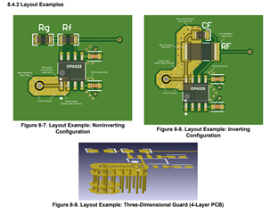
I'm open to hearing any ideas of what I could be doing wrong, including other explainations of the higher cut-on frequnecy aside from the large resistors being shorted out by a leakage path. I also included the layout of my PCB below (Figure 4). Thanks

Figure 4

  • Hey Xiya,

    Do you know the insulation resistance of the capacitor you are using? This will usually be in the capacitor datasheet. Typically this will be high for low value capacitors, so this may not be the case.

    Just adding 100MOhm of parasitic capacitance shifts your passband frequency to about 1kHz

    Are these measurements after cleaning off the soldering flux from the board? Flux contamination may not have a consistent leakage resistance value, but could be the cause of this. I would try cleaning the board with isopropyl alcohol and re-measuring to see if the same passband is seen.

    Best,
    Jerry

  • Hey Jerry, thanks for your reply! Capacitor insulation resistance was one of the first things I checked for too, and all of the datasheets I found for my parts look similar to the one you posted, where they should be in the gigaohms range, not the <10 megaohms that seems to be causing the cut-on frequency shift. Additionally, I tested configurations with 2pF, or 10pF, or 820pF capacitors all from different manufacturers in the feedback loop, and all of the circuits exhibit a similar cut-on frequency shift, which corresponds to the capacitor value I used, and a ~2MOhm parasitic resistance in the feedback path. The consistency of the value of the paraistic resistance makes me think it must not be the capacitor's leakage resistance.

    You are right to suggest cleaning the board as well. I am currently cleaning it by brushing the entire board with IPA using a paintbrush after all the components have been reflowed onto the board, but I'm not sure if there are any additional steps I may take to clean it better. I've tested cleaned and uncleaned boards, and they have similar shifts in cut-on frequency (~100x).

    Currently my suspicion is on the board material being faulty, or my PCB design making it too easy for current to bypass the large resistor, or somehow the leakage path is inside the op amp itself between the inverting and output terminals (very unlikely).

    I read online many places I should have a guard ring around the high impedance nodes of an op amp, like the inverting terminal of the op amp in my circuit, but I am not very sure of why or how that could totally solve the leakage problem, or what was causing the 1-3MOhm leakage resistance in the first place.

    I've been pulling my hair out over this problem for the last week and a half, so I appreciate any ideas or input on this topic. Thank you very much

  • Hey Xiya,

    If you want to isolate the board parasitics, you can try to air-wire the feedback path. This would involve bending up the IN- and OUT pins of the IC, and soldering a small wire and the feedback components to those leads (see below picture for air-wired input pins). As long as you make sure the terminals are not touching the board you can isolate the possibility that it is board parasitics.

    I believe the procedure you have taken for cleaning will be sufficient.

    Best,
    Jerry

  • Hi Jerry, thanks for your reply! Air-soldering is definitely an interesting idea and I will try that next. My only conern is, my feedback components are all chip mount and very small (0805 package size), so I am not sure of how feasibile the task is of trying to solder them in air to the short wire leads.

    I will keep you updated if the air-soldering works, and in the meantime if anyone here has experience on using guard rings for high impedance applications such as this, please inform on whether or not redeisgning with a guard ring around the IN- node would potentially solve this issue. My proposed location for the guard ring is in the image below, drawn in black. It would have the same potential as the IN+ node (connected directly to gnd), and thus would draw in and stop any leakage that's trying to bypass the 500MOhm resistor to get to the OUT node.

    I know this circuit design can work, as I've read at least 2 PhD dissertations which employ a very similar circuit with even larger resistance values in the feedback path (>1G Ohm) for the same application, getting a cut-on frequency which corresponds to the resistor value used, instead of a low value leakage resistance. I just want to figure out exactly what I was doing wrong, so any input is appreciated.

    Thank you very much,

    Xiya

  • Hey Xiya,

    Let me ask my coworker who specializes in PCB layout for his recommendation on guard ring implementation. However, he is out of office for the rest of today and tomorrow, so I will get an answer to you on Monday.

    Best,
    Jerry

  • Hello Xiya,

    I suggest using a much lower resistance then use a second amplifier to boost the AC voltage. 500M is very large and 2pF is very small.

  • Thank you so much Jerry, that would be great! I did some more testing today and it looks like another potential cause for the leakage is the water-soluble solder paste I am using, which leaves some conductive flux (<10MOhms on multimeter) on the underside of the surface mount 0805 components I am using, and it is almost impossible to clean after the components have been soldered onto the board as they are covered by the components. 

    I ordered some no-clean solder paste today, so by the time they arrive I will be able to perform some more tests. The guard ring though is something I hope to understand better, so any information on them would be great, especially for analog operations such as this.

    Thank you again!

    Best,

    Xiya

  • Hey Ron, thanks for your reply! That's a great suggestion and it's definitely the backup plan I will use if all else fails. The reason I didn't just opt for using higher capacitance and lower resistance is that it will increase the output-referred noise of the entire circuit, and thus also increase the minimum detectable pressure of the piezoelectric sensor + PCB setup. I also want to exhaust all of my current options before changing the design of the PCB board itself, which will need to be fabricated and shipped, which costs lots of time and money. Thank you again for the suggestion though, I really appreciate the input.

    Best,

    Xiya

  • Hi Xiya,

    Perhaps the best articles for guard ring design come from Paul Grohe's 3-part series on low leakage design, linked here: https://www.edn.com/design-femtoampere-circuits-with-low-leakage-part-one/

    The black guard ring you have placed on your PCB design would be a good implementation of a guard ring around the sensing node, but be sure to include the input trace connected to TP2.

    Here is an example layout using our OPA928


    The most important factors to consider/verify:

    1. Ensure you are fully encircling all components connected to the inverting node of the amplifier.

    2.  If you are not using a device with a dedicated guard ring driver, use another channel of the amp, or a separate amplifier to force this guard voltage on the ring.  

    3. Board cleanliness is incredibly important to ensure low current measurement. 

    4. While not necessary in all applications, removing the soldermask around the low current area can further remove sources of leakage to the PCB substrate.

    5. it is a good idea to guard any area which is connected to the inverting input, this certainly extends to through hole components. In the case of a two layer board, I would guard on both layers if the input signal passes into a TH connector. A via fence around the guard ring can also help reduce any leakage paths through the substrate of the PCB.

    This is how I would design the guard ring for your board:

    Again, connect the guard ring to a driver to ensure the guard ring is driven to the correct voltage. 

    I have been able to see good performance for leakage current even using FR-4, but eventually you will likely need to use more exotic materials like Rogers 4003C for ultra low leakage. 

    Another way to further improve low current sensing is to create multiple guard rings on other layers of the board. Leakage does not necessarily work exclusively in 2D, considering the 3D leakage path can be important to get the best performance. I have designed boards where I guard the layer directly underneath the guard trace to prevent leakage currents from going down into the PCB. Figure 8-9 of my included picture shows this theory well.

    Please feel free to make changes to the PCB and resubmit them to this thread for review. I am happy to review your changes.

    Thanks,

    Jacob

  • Hi Jacob, thank you for the incredibly detailed and well thought out response!

    I am currently working on a second design of my charge amplifier circuit and have already implemented some of the things you suggested, such as extending the guard ring all the way down to the input pad. I will certainly send the new design here once I'm done with it, and would greatly appreciate a second set of eyes to review it.

    I have pretty much figured out what the original issue was caused by, for anyone who's been following the thread, it was the solder paste I was using, which uses a "water-soluble" flux, instead of a "no-clean" one. This means that the flux my solder paste left behind was both conductive and corrosive, and since I used small surface-mount components, there was still a considerable amount left on the underside of the components even after brushing the board with IPA, which was enough to create a <10MOhm leakage path. For anyone designing circuits which require a high impedance, please remember to check that the solder paste you use is classified as "no-clean", because otherwise the flux residue may be conductive on the order of 10s of MOhms or less, and it could screw up your design.

    It turned out to be a wild goose chase for a pretty simple issue, but I am very thankful for the experience, as I got to learn a lot about the different ways leakage could occur on a circuits board, as well as design decisions one could take to minimize it (i.e. proper guard ring implementation). Thank you again to everyone who replied and offered their help to me in this thread, it would've taken me a lot longer to find the root cause without the valuable guidance.

    Best,

    Xiya

  • Hi Xiya,

    Great to hear that you solved the issue! I have almost exclusively used no-clean flux in the past, but I am glad that you shared your results for the water soluble flux. I will be sure to add this to my list of notes for low IIB measurements.

    Thanks!

    Best,

    Jacob