This thread has been locked.

If you have a related question, please click the "Ask a related question" button in the top right corner. The newly created question will be automatically linked to this question.

PGA308EVM: One Wire Calibration Connections PGA308EVM

Part Number: PGA308EVM
Other Parts Discussed in Thread: PGA308, , XTR116, PGA309

Tool/software:

Hello,

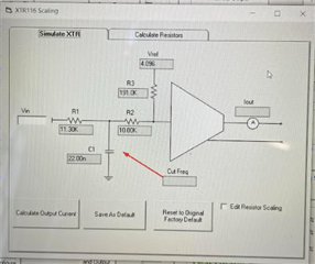
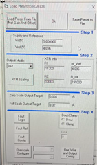
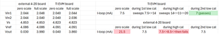
I am looking for help verifying connections for the "one wire" calibration method.  For the attached circuit (figure 6-3 of PGA308 manual), I don't see any explicit guidance in the manuals and would like to verify the following hardware connections/settings for writing calibration gains to the PGA308. 

T4 (Vout_F) to "one wire or Riso of circuit.

T4 (ground) to Iret of circuit.

T1 (Vref Ext) to 4-20 high of circuit.

T1 (Ground) to 4-20 low of circuit. 

  • Ryan,

    I am working on a comprehensive answer to your question.  I will get back with you tomorrow.

    Art

  • Ryan,

    Attached is a step-by-step guide on how to calibrate using the PGA308EVM.  This calibration procedure makes use of the built-in sensor emulator.  You will need a +/-15V supply, a floating 12V supply, and a 9V supply.  Once you have done the calibration with the sensor emulator successfully, I can help you with your real-world sensor and/or your sensor module.

    pga308EVM-Current Loop.pdf

    I hope this helps.

    Art

  • Art,

    This is very thorough and helpful.  We really appreciate the help.  This looks like a great guide for this specific case.  I'll run the emulator calibration and will be following up for guidance on calibrating my real world sensor module. 

    Best,

    Ryan  

  • Art,

    I made it through page 12 steps and get an error message "Zero DAC is out of range: -2.5<Fine_Gain<2.5" and sometimes "Fine Gain Out of Range: Fine Gain Range: 0.33333<Fine_Gain<1.0000"

    I am connected identical to pages 5 and 6 with the exception of the 9V supply and 12V floating supply using different outputs of the same power supply.  The floating supply and INA power are isolated to separate power supplies.  I noticed your bottom meter on page 6 is reading 14V.  Is the target +-12V here?

    I double checked all of the jumper settings. 

    I'm running approx. 15mA on the ammeter during cal and approx 25mA after cal. 

    Any suggestions?  Thanks for the help!

    -Ryan 

  • Ryan,

    • I think the problem is the "9V supply and 12V floating supply using different outputs of the same power supply.".  This may or may not work depending on the supply.  In some power supplies the ground of the different channels are tied together and for other supplies the channels really are floating relative to each other.  If you have an extra power supply I think it would be good to use a seporate supply for these two items.  Note that the +/-12V supply and the 9V supply don't have to float from each other, so maybe you can just rearrange your connections.  
    • The actual voltage that each input requires is a range of voltages.
      • T2 - The connections labeled +/-15V on the USB-DAQ-Platform could range from 12V to 16V (I used 14V)
      • T1 - The connection labeled +VL an -VL are the loop supply.  This needs supply needs to float.  This voltage could range from 12V to 24V.  I set it to 12V in my experiment.
      • T3 - The 9V input can range from 6V to 10V.  This was originally intended to be used with a "wall-wart" (wall power supply ).  That supply was removed from the EVM kit at some point, so now you need to find an additional supply or purchase a wall-wart from digikey or other.  I used a 9V wall-wart.
      • no other external connections are required.
    • The Zero DAC out of range and/or the Fin_Gain out of range happens when the calculated sensor output span and/or offset is too large to correct for.  The calibration algorithm calculates the sensor voltages by taking the PGA output and dividing by the gain.  So, if the PGA is not operating properly (e.g. it its output is saturated), the software calculates incorrect values for the sensor output and the algorithm says that it cannot correct these large errors.  This error could also happen if the sensor output are truly too large.  I set the simulated sensor outputs on page 11 to 0.5m and 5m.  This is the normalized sensor outputs so the sensor output voltage is 0.5mV/V and 5mV/V multiplied by the excitation voltage.  You should double check this to make sure you entered these numbers correctly.  Note that the units "m" need to be lower case for milivolt.  This software is case sensitive so it needs to be lower case "m".
    • You should double check the jumper settings.  It only takes one incorrect jumper setting to make the calibration fail.
    • I can't think of any other suggestions.  If these suggestions don't help, we may want to do a webex / phone call.

    best regards,

    Art

  • Art,

    Thank you for looking into this, we certainly appreciate it.  I'll isolate the 9V and 12V supply as well as do all of the recommended settings and jumper checks.  Hopefully we find something obvious!  I won't be back in the lab until tomorrow but will follow up ASAP.  It's encouraging to know we can do a call if we need to.

    -Ryan 

  • Ryan,  Happy to help and looking forward to hearing your results.

    Art

  • Art,

    Great news, we ran a successful 4-20 cal on the internal chip and are ready to write to our external chip.  I isolated the 12V and 9V with no change.  It turned out to be that my +14 and -14 source ground termination was incorrect.

    Our external circuit is identical to figure 6-3 above.  Can you assist with similar guidance for writing calibration gains to that chip?

    Best,

    Ryan 

  • Ryan,

    I think you want to connect your own sensor module and program that module ( as us shown in the image below).  This document shows how to do that:  Connections to custom sensor module

    I hope this information helps!  Best regards, Art

  • Art,

    Thank you, this certainly helps!  We're just about done in the lab for the week and will give Option 2 a go when we pick up next week.

    This looks pretty straight forward for the most part.  I assume there are software settings I'll need to adjust.  Specifically the one wire control within the load preset tab? (image below)

  • Ryan,

    • Step 2 in the calibration tab of the software is currently configured as "Use DAC Signal".  You should change this to "Apply signal externally"
    • Step 3 - Eventually, you may want to select an external meter.  For now I would just use the USB DAQ A/D (keep this option the same for now).
    • Step 4 - Keep the pre-cal file the same.  Any changes you make to the one wire signal should be done in "post cal".
    • Step 5 - this is really irrelevant now.  The numbers here are used for the sensor emulator and you are not using that now.
    • Step 6 - the software will pause at each key calibration point.  You will need to adjust your sensor stimulus (e.g. pressure, strain, etc..) each time the software pauses.  The down arrow means adjust to minimum and the up arrow means adjust to maximum.  The software will calculate the sensor output based on the PGA gain, offset, and output voltage.
    • Step 7 - this is currently disabled.  You may want to enable this if you want to configure the one-wire differently for normal usage of the sensor module.  For example, you may want to use OWD to disable the one wire interface.  Other things that may be different in postcal are the usage of the overscale/underscale range and/or clamp feature.  These features should be disabled during calibration but can be enabled once the calibration is complete.  Be careful about using OWD OFF as this will permanently disable the one wire interface.  The main reason for adjusting the one wire configuration is to prevent inadvertent communications with the device after it has been programed and is acting as a sensor module.
    • Step 8 - you may want to program the PGA308 once the calibration is done.  This will write into bank 1 of 7.  Once this is done you can cycle power and the PGA308 will retain the calibration settings.  You can reprogram up to 7 times.  After the 7th OTP write, you cannot reprogram further and you will have to desolder the PGA308 and replace with an unprogrammed device. 

    I'm glad you are making progress.  Best regards, Art

  • Art,

    We really appreciate the detailed and thorough help!  

    I'll give this a go later this week when I'm back in the lab and follow up.

    Best,

    Ryan 

  • Ryan,

    Thanks!  I look forward to hearing the results.

    Art

  • Art,

    Okay so not quite there but made more progress.  Getting the error message "Fine Gain Out of Range: Fine Gain Range: 0.33333<Fine_Gain<1.0000" after applying upper limit to sensor (full bridge load cell).  Can you help verify my variable (4) below and look for any other suggestions?  Thank you! 

    Sensor module connections: connected my sensor module (containing XTR116, PGA308, and other components identical to figure 6-3 above), using page 11 connections to J3

    Sensor connections: double checked and wired via module output diagram

    DAQ power connections: double checked and wired via page 10 connections  

    DAQ jumper settings: double checked and wired via page 5 settings (same as internal settings from before)

    Variables I'm looking into: 

    (1) My sensor bridge resistance/span/gain are within PGA308 tolerable ranges.  Currently using a small puck style 250lbf full bridge load cell with a nominal gain of 2.0+-1% mV/V, an input impedance of 750ohm, and an output impedance of 700ohm.

    (2) Ensuring exact application of load to puck.  Was using weights in the lab which were only approximately 2/3 of sensor capacity but consistent.  I assume this is okay for a proof of concept, giving an inaccurate mA/lbf output, but okay for just initial go-no go system checks.  I did run a cal with the sensor disconnected and received the "Zero DAC is out of range: -2.5<Fine_Gain<2.5" so I know the sensor is being seen by the 308.  I did make it through cal at one point to the second low point step and then errored out on that step.  The DAQ measures the upper limit @ 18.76mA and lower limit @ 18.77mA which doesn't make sense.  

    (3) Verify sensor module board traces and pinouts/footprints match figure 6-3.  I've double checked these but will check again.  The sensor excitation is correct and 4-20 loop is running in the right ballpark.

    (4) Verify the XTR Scaling tab within the load presets tab does or does not need to match sensor module circuit.  I changed these component values from default to match the sensor module circuit with no change either way.  Images below.

    Default Settings:

    Modified Settings To Match 6-3 sensor module:

    Error message and outputs:

  • Ryan,

    Thanks for the excellent notes.  I hope we can resolve your issue quickly.

    1. Do you know the sensor offset?  The sensor span is 2mV/V.  With a 4.096V reference this is approximately 8mV full scale.  Some sensors have very large offsets (e.g. the outptut would move from 10mV to 18mV.  For some of these unusual cases, the PGA308 may not have enough correctoin range.  I doubt this is the case, but if you can measure the raw sensor zero-scale output and full-scale output that would be helpful to confirm.
    2. Once you can tell me the measured zero and full scale sensor output I can emulate that condition to make sure the PGA308 can calibrate that sensor output range.
    3. Based on the last image, I think there is a hardware issue.  The measured offset and measured full-scale read the same.  This tells me that one of the following is probably true:
      1. The sensor is not connected to the input or the sensor excitation is not connected.  Can you measure the raw Vexc and sensor outputs on the PGA308 input pins.
      2. The PGA308 output is not connected to the XTR, or the XTR has incorrect resistors for the sailing options.  When I look at my PGA308 schematic, the resistor values are different from my software.  So, I need to go into the lab and measure what is actually populated and make sure that the software matches the actual circuit.  It looks like you already did this verification.  I think the algorithm would work ok even if the resistor values were not correct as long as they were in the proper range.  This is true because the calibration algorithm corrects for gain error.  There is a limit to how much correction it can to so Ideally these resistors would be the same in software and hardware.  I don't think the error in your case could be from a small difference between the software and hardware values for these resistors.  The reason it needs to be a very significant issue is that the result is the same for zero-scale and full-scale.
      3. During calibration, you should include a debug ammeter in series with the current loop.  As the load is adjusted and the calibration procedure proceeds, you should see variation in the 4mA to 20mA.
      4. The PGA308 is communicating, so we know the XTR powers the device and it is basically functional.  So the question is why does the output stay at only one level.  If possible you should monitor Vin1, Vin2, Vs, Vref, and Vout on the PGA308 during calibration.   Does Vout stay at one specific value?
    4. Another possibility is that the software is not configured correctly.  This seems unlikely to me as the settings should be almost identical for the EVM with sensor emulator test and the sensor module test.  If the debug above doesn't yield any good results, you could wire your sensor to terminals T5 and T3 on the EVM.  Thus, you would be using your actual sensor, but the PGA308EVM Test Board for the PGA308+XTR.  If this test works, than the issue is the difference between the EVM and your PCB.

    I hope this helps!  Best regards, Art 

  • Art,

    Thank you!  This is becoming quite the long support thread for you and we really appreciate the help.  I won't have time back in the lab until Monday but will start following up on these now for a placeholder.  I ran through all of the PCB traces, datasheet pinouts, and component placements with no problems found. 

    1: Sensor offset is listed as <1% of rated output (~8mV like you mentioned) so calculation yields a very low 0.08mV.  Will follow up and measure this in the lab.

    2: Will follow up and measure this in the lab.

    3a: Vexc was running right at ~4.096V (measured), and didn't get a voltage across Sense+ and Sense- which I guess would mean offset is low. Will follow up and measure this in the lab and verify Vexc at the actual 308 (pin 10 Vref) as well as grab 308 output voltage from 308 (pin 9 Vout).

    3b: I measured/configured these both ways with same error but will certainly not lose sight of this as calibration develops.

    3c: Original results on the ammeter yielded strange values; sometimes would drop to ~7mA for both low and high cal points and then ~18mA for both high and low on other runs...couldn't make sense of it.  Will follow up and measure this with actual values.

    3d:  Will follow up and measure these in the lab.  I would be mostly curios about Vout as well...

    4:  Great idea with using the EVM board as troubleshooting logic!  I'll give this a go if all else fails above.

    Thanks again and I'll plan on following up Monday.

    Best,

    Ryan 

  • Ryan,

    I provide one short response, and wait for you to do further measurements:

    The way the calibration algorithm works is that it initially sets all the gain values to minimum gain, and all the offset values to try and force the PGA output to mid scale.  Thus, if the PGA309 input was 0mV the output would go to 12mA (mid scale for a 4mA to 20mA transmitter).  On the other hand, if the input is 1mV, the output will move to something like 12.5mA.  In both cases the calibration algorithm can then calculate the input voltages based on the output, gain, and offset settings.  Once the PGA309 input is known for minimum and maximum pressure (strain or whatever stimulus), the gain and offset can be adjusted to achieve the desired output range (4mA to 20mA).  The key point here is that you should expect to see outputs in the 12mA range at first while the algorithm determines the input.  Below is the algorithm math details.

    PGA308_calibration_procedure.pdf

    Best regards, Art

  • Art,

    Thank you, this logic will help me run through diagnostic measurements as I'm debugging.

    I'll be back in the lab tomorrow and will hopefully be responding back with something definitive!

    Best,

    Ryan 

  • Ryan,  Excellent.  I look forward to hearing the progress.

    Art

  • Art,

    Okay so I made some progress but still fail with same "Fine Gain Out of Range: Fine Gain Range: 0.33333<Fine_Gain<1.0000".

    Responses to measurements/questions:

    1: Sensor offset is 8mV.  measured zero scale = 0mv full scale = 8mV

    3a: raw Vexc @ pin 10 on the 308 is 4.086 which matches sensor Vexc at connector.

    3b: image below, adjusted to external module circuit.

    3c: amperage (I didn't get good results here and may need to reconfigure my meter, levels fluctuated around 1-1.5mA which doesn't make sense)

    3d: (value = zero scale-full scale): (Vin1 = 2.044-2.048), (Vin2 = 2.044-2.040), (Vs = 4.853-4.853), (Vref = 4.086-4.086), (Vout = 0-3.990)

    4: Sensor "passes" calibration using EVM board but automatically switches the output mode to Vout.  (image below).  Is it possible that I'm missing a software setting somewhere for scaling to my sensor module instead of EVM?  Images below 

  • Ryan,

    On Oct 11, you mentioned "Great news, we ran a successful 4-20 cal on the internal chip and are ready to write to our external chip.".  I think used an older version of the PDF below to do the setup.  I ran through this again today and added a few slides, so the updated file is given below.  The update was to add a few slides about programing OTP.  When I ran through this procedure, the software did not switch back to Vout mode when I finished.  Even after closing the software and opening it again it retained current mode.  When I did my calibration I set the sensor emulator to output 0mV and 8mV.  When I completed the procedure I programed OTP, cycled power, shut down software, and restarted the software.  After the restart, I was able to get 4mA to 20mA with 0mV to 8mV input.  The last slide in the presentation shows the gain and offset values that the PGA308 was set to for your input signals.

    I notice that you have "load post cal" check-box checked.  I think this may be the issue.  The purpose of this feature is to select a post-cal configuration that enables features that should be turned-off during calibration.  For example, during calibration you do not want over-scale or under-scale enabled, because that may limit your output range which could impact calibration results.  This feature can be enabled after the gain and offset values are determined using the "load post cal" check box.  In your screen-shot you don't have a file selected for post cal.  I think it is likely that a voltage output mode post cal is being selected and that is what is causing the issue.

    Can you repeat the basic calibration outlined in the PDF below with the "Load post cal" checkbox unchecked?  When you do this you can set the sensor outputs to 0mV and 8mV (in the location marked Step 5b).  When you step through this you should get very good post calibration accuracy.  Also, you should not see the calibration mode switch to Vout mode (it should stay in current loop mode).  You could program the OTP and you should see that the values retain after cycling power. If you get all the expected results, then you can go back to your external sensor.  If you get the out of range message in this case, than you have a sensor issue or a wiring issue.  You should use a volt-meter to verify the input signal if you don't get the expected results.

    Sorry for the difficulties you are having.  I hope we can resolve them quickly.

    Best regards, Art

    pga308EVM-Current Loop-10-24-2024.pdf

  • Art,

    Thank you, I really appreciate the detailed help.  This is encouraging!  I was really hoping it could be software related as I've triple checked the PCB, components, and wiring.  

    One question:  Do I configure the block diagram settings to the same settings shown on page 7?

    I'll be back in the lab in the morning and will run through these scenarios.  I loop back with my results.

    Best,

    Ryan 

  • Ryan,

    You should not have to configure the block diagram at all.  The pre-cal file and calibration process will do all the configuration.  The block diagram is really most useful as a way to see what the calibration process did.  Technically, you could select "Run out of RAM" mode in the lower left corner and then you could manually adjust the different gains and offsets for the PGA308.  I really never do that thought, as I generally let the calibration choose the values for me.

    Best regards, Art

  • Art,

    Thank you, I ran again this morning with mixed results.

    Excluding the load post cal feature I was able to calibrate and measure post cal results successfully and accurately with the EVM board connected to my load cell, and not revert to Vout settings.  So we're good to go there as far as software settings go there.

     Unfortunately when connecting the external 4-20 board configured identical to figure 6-3 on page 78 of the PGA308 manual we still fail with the same fine gain error.  Something is going on with my current loop.  Measurements of the EVM vs external 4-20 are as follow.  Voltages look nearly identical, while the current is not.  I think at this point I'm leaning towards my XTR being damaged/faulty or capacitors being misplaced.  I'm going to layup another board with new components to rule this out.

    I'll loop back with results once I layup a new board and test. 

    Thanks again for the help!  Hopefully this will be the missing link. 


  • Art,

    No luck with swapping components.  Swapped the XTR116, capacitors, and BJT with new and correct value components and have the same results as listed in the table above.  A few questions listed below.

    1: Is it possible the PGA chip is damaged and still has the correct voltage outputs above?   I'm going to start laying up an entire new board to verify that.

    2: Are there specific jumper settings on the DAQ that need to be changed when switching from the EVM board to the external 4-20 module?

    3: Are there specific software settings that need to change when switching from the EVM board to the external 4-20 module? 

    The calibration passes when sensor is connected through the EVM board but fails with fine gain error when the EVM is replaced with the external 4-20 module.

    Best,

    Ryan 

  • Ryan,

    • Please use the document below (custom connections), when deciding how to make connections between the USB-DAQ-Platform and your module (slides 10 & 11).  Figure 6-3 is correct, but the document below shows the specific EVM connections needed.
    • Can you take a picture of your setup.  Show the USB-DAQ-Platform connections and the connections to your sensor module.
    • The PGA308EVM schematic current loop section shows an incorrect value for R21.  R21 = 11.3k, R11 = 10k, and R22 = 191k.  This is reflected correctly in the software, so the circuit works well.  The schematic shows R21 = 15k, but the EVM and software use R21 = 11.3k.  The key point is to confirm that your circuit matches your software configuration.
    • Your input signals look correct for both cases.  This is good information because we now know that the input is correct.  Also, we know that the PGA308 is capable of calibrating the range you are using successfully.
    • I think the V-to-I translation must have an issue on your circuit.  Please check the following:
      • Confirm that the schematic matches the PGA308EVM schematic for the current loop.  If you send me your schematic, I can check it as well.
      • Confirm that your software setup for the resistors on the XTR matches the actual resistors.  I recommend just using the default values given in the software (R21 = 11.3k, R11 = 10k, and R22 = 191k).
      • Confirm that you are using the XTR116 (4.096V reference).
      • The XTR116 scaling tool in the EVM software allows you to calculate the output current given different inputs.  Use this tool for the two output signals you have 0.04V and 3.86V.  I did this and got 2.3mA to 20.27mA respectively.  You should get these two output currents for your circuit.  If you don't the XTR is not wired correctly (see calculation tool below).
    • If your schematic matches the EVM schematic the circuit should work.  I common issue with current-loop designs is that the Ireturn is connected to a non-floating ground.  Using the XTR115 with the PGA309 to Generate 4mA to 20mA Output explains the grounding considerations.  Please review this document and your setup to see if you are doing something incorrect with grounding.
    • I hope this helps.  We just need to figure out what is different about your V-to-I circuit.

    7140.pga309-USB-DAQ-connectipon-to-custom-sensor-module.pdf

    best regards, Art

  • Ryan,

    If you like, send me an E2E friend request so that we can switch to email, and set up a meeting.  I think a call might be the quickest way to debug this issue.

    Best regards, Art 

  • Art,

    Okay great, I appreciate it!  A call might be best.  I sent a friend request and I can put together the responses to your last thread realistically on Monday when I'm back in the lab.

    -Ryan 

  • Ryan,

    I just sent you and email.  Please let me know when you want to set up a call.  Let's close out this E2E thread.  We can move to direct email and phone calls.  I really thing you are very close to getting this to work and the call should take care of the last few details.

    Art

  • Art, 

    Okay thanks!  I'll follow up via email.

    -Ryan