This thread has been locked.

If you have a related question, please click the "Ask a related question" button in the top right corner. The newly created question will be automatically linked to this question.

OPA392: Measuring current noise of a current source?

Part Number: OPA392
Other Parts Discussed in Thread: TINA-TI, OPA334, OPA375, OPA344, OPA2375, TLE2426

Tool/software:

Hello,

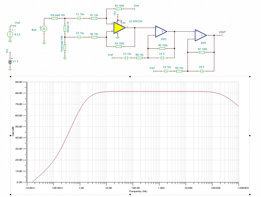
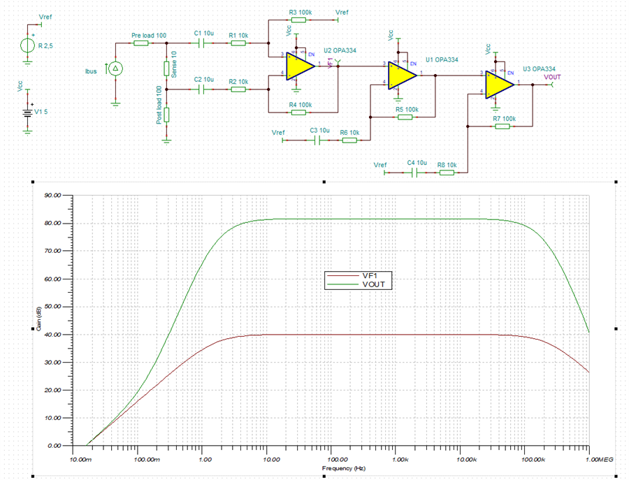
I built a current source using this circuit.

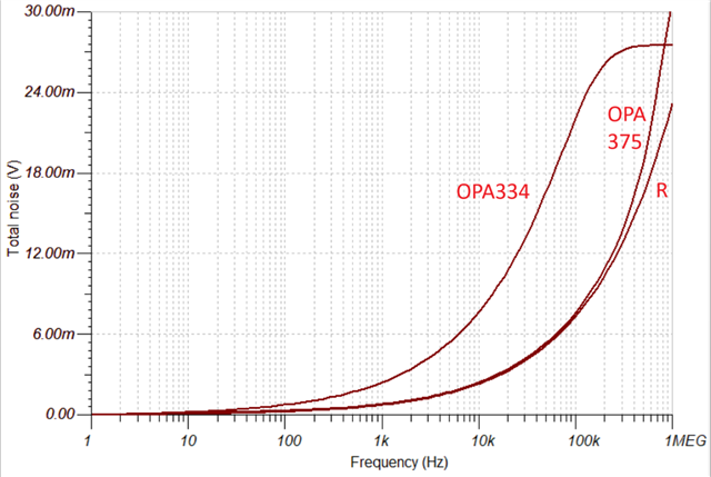
According to the simulation, the current noise is about 3 uArms ("total noise" in Tina-TI, analysis from 1  to 10 MHz) with a maximum current noise density of about 30 nA/RtHz ("output noise" in Tina-TI).

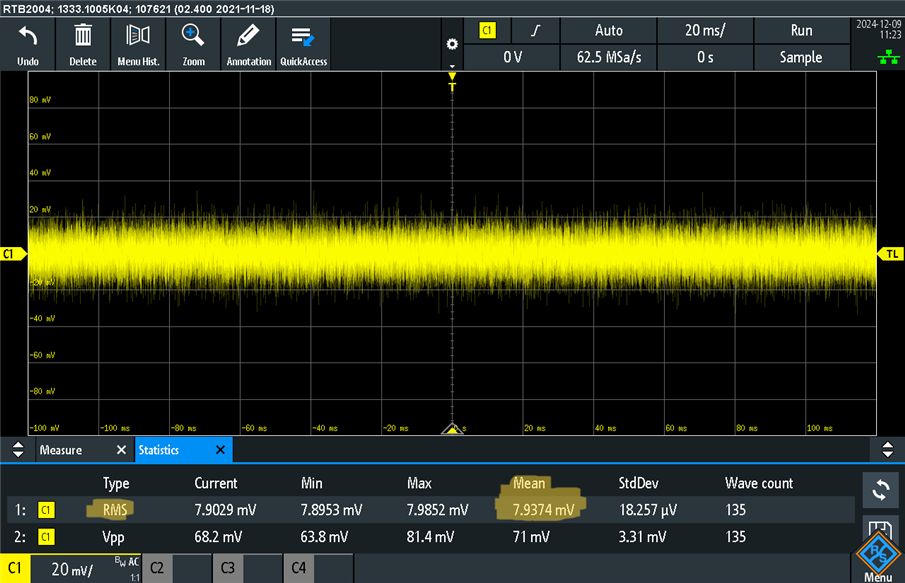
Now I want to validate the real circuit and measure the current noise of if.

How do I do this?

I cannot simply use a difference amplifier and a shunt as I want to measure the AC component and disregard the DC component of the current.

Further, I understand that I will need a spectrum analyzer to measure noise density.

To get started, it will be sufficient, though, to just measure the total RMS noise. Would a oscilloscope suffice for that measurement?

Thank you and have a good weekend!
Dan

  • Hello Daniel,

    You could read current noise by reading voltage noise across a resistor that is in the current path.  

    Direct oscilloscope noise measurement usually is only good for high noise level because the shorted input baseline noise is rather high on most scopes. This baseline noise can be reduced by using shielded direct cable. These cables are capacitive at frequencies below transmission line. The 20MHz BW input scope filter helps reduce bassline noise.

    Using a low noise preamp between noise source and oscilloscope is recommended. 

  • Dear ,

    Thank you for your immediate response. I admit that I struggle to put your comment to practice.

    I can test my design with a 10 Ohm shunt resistor in the current path. With the noise values given before, I expect the measured noise signal to be in the range of 30 uVrms. With this said, I'd need a gain of about 1000 to get an appreciable signal on my scope.

    I assume this amplification could be achieved using a difference amplifier, see my link in my first posting or again here: link

    Now how do I go about measuring the AC (i.e., noise) component only and blocking the DC component? I cannot just connect this difference amplifier across the shunt resistor as it would also amplify the 1 V signal from the 100 mA DC current and saturate the amplifier. Do I connect the difference amplifier circuit using capacitors to block the DC component? I think that a 10 uF capacitor would form a high pass with the resistor (from the resistor divider at the input of the op amp, about 100 kOhm) and this would (hopefully) give a cutoff frequency of 1/(2*pi*10uF*100 kOhm) = 150 mHz. But it doesn't in my simulation:

    This is what I hoped to achieve with this simulation: VG1 should simulate the noise voltage across the shunt resistor in the current path. The AC analysis should show that DC is blocked but frequencies above about 1 Hz should be amplified by +60 dB. That did not work out. The gain is stuck at -23 dB. The Tina TI file is attached below. (Note: The screenshot above shows C1/C1 as 1uF instead of 10uF but that does not change the result considerably).

    Please elaborate on how to properly connect the "low noise preamp" to the shunt resistor. Thanks.

    Tina Ti File: 16 AC coupled difference amplifier.TSC

  • Daniel,

    Like this. the firs stage is AC coupled diff amp (pick low noise amplifier) that can work low or high side connected. Extra (1 or 2) stages increase gain. 

    The output should also be measured as AC coupled. Feel free to change component to reduce the lower cutoff off frequency. It is 3Hz as drawn. 

  • Dear ,

    Thank you for your suggestion.

    I tried to simulate your circuit in TIna-TI and I

    • limited the circuit to the first of the three amplifier stages
    • selected OPA334 (as it is one of the amplifiers with the lowest input offset voltages that I could find)
    • started with a DC coupled amplifier (to see if that works as expected in DC operation).
    • replaced the current source and resistors of the input stage with a voltage source VG1 (that mimics the voltage noise directly)

    When I set the voltage source to 300uV, everything is as expected: the op amp's inputs are balanced, the gain is 20 dB and the output is 3 mV.

    However, when I reduce the voltage source to 30 uV (which is the expected noise voltage according to my estimation, see my second posting), the gain collapses and voltages at the op amp's inputs differ:

    Why is this? Should I choose a different op amp? Please help. Thanks!

    Please find the simulation file attached: 20 DC coupled difference amplifier G=20dB.TSC

  • Daniel,

    The problem is the DC operating point setup. Output DC is at the negative rail (0V), that is not a linear operating point.

    Here is my circuit with OPA334 put in 1st slot.

    In in work.TSC

  • Hello ,

    Thanks for providing your Tina-Ti file. That was really helpful.

    Of course, your circuit looks like it does what I tried to accomplish:

    I fiddled with your circuit and replaced the unnamed op amps by OPA334 (and also removed C5 and C6 as they were 0). T

    This did not change AC transfer characteristic (green curve) considerably, except for the upper frequencies where the OP334 stages roll off earlier. Should I use a different op amp for the second and third stage, instead?

    Do you have any suggestions what to look out for when creating a layout for your amplification circuit?

    Thanks again.
    Dan

    Tina-TI: 31 ti.com with 3x OPA334.TSC

  • Dan,

    C5 and C6 can be used to reduce bandwidth. Less BW is less total noise. A low value like 10pF improves phase margin.   

    Now would be a good time to consider the noise of the amplifier circuit. You can divided by 81dB to get input referred noise level. 

    Perfect op amps would just have the resistor noise "R" ; with OPA334 you get a lot more noise. OPA375 is a much better choice.

    If you need better noise than this then you need lower value resistors.

    For layout keep feedback resistors close to amplifiers. Don't run output trace close to input to avoid unwanted feedback. Add supply bypass capacitors on each op amp and include a ground plane.

  • Hello ,

    Thank you for the additional information.  I'll keep a footprint for C5/C6 in any case.

    I have three topics where I kindly ask you to weigh in.

    Regarding op amp choice, you are suggesting OPA375 instead of OPA334. Do you suggest to use OPA375 for the 2nd and 3rd stage only or in all amplifier stages? And what properties of the OPA375 made you select it for this application? I chose the OPA334 as I was under the impression that a low input offset voltage is paramount when measuring small voltages as the input offset voltage would add a significant error to the small voltage I want to measure. OPA375's input offset voltage is specified as max. 500 uV, whereas OPA334 has an input offset voltage of 5 uV specified. However, this circuit is about measuring AC voltages, so the value of the input offset voltage parameter might be irrelevant. Is is correct that the input offset value can be ignored when measuring the RMS value of an AC signal?

    Regarding total noise value, I was able to re-generate your graph using TINA-TI's  by simply running "noise analysis". It is my understanding (learned from here: link) that TINA-TI's "Total Noise" plot is to be read as follows: for the summed RMS noise from the analysis start frequency up to a specific x-axis value, read the plot y-value at this specific x-axis value. So up to about 500 kHz, the OPA375 is highly superior, but taking higher frequencies into account, the OPA334 total noise is lower compared to OPA375 (as there total noise plot for OPA334 crosses the plot for OPA375). How do I properly interpret the total noise graph and what should I use as upper frequency to read the total noise value (as this upper frequency will have a big impact on the resulting total rms noise value).

    Regarding gain plots, the gain plots seen above are created in TINA-TI by simply running "AC analysis". I assume this will give me the closed loop gain. I noted that in other cases one had to first modify the circuit (i.e., "break the loop") and then run an AC analysis of a circuit in TINA-TI, for example see this discussion (link), What is the difference? Does "breaking the loop" give me the loop gain which is required for stability analysis?

    I appreciate your insights very much.
    Thanks.
    Daniel

    PS: Edited...

  • Daniel,

    For first stage OPA375 helps a lot ; for each sequent stage it is less help. Vos is a DC value that create a DC offset that only affects DC performance. Noise is entirely AC. So DC does not matter. C1 and C2 throw away all the source DC. 

    The only reason OP334 noise appears to stop rising it that the OPA344 forward gain is falling at a fast rate (so it is not amplifying the highest frequency signal nor added noise). OPA334 has less bandwidth. I forgot if you mentioned a upper frequency of interest. 

    In schematic the forward gain (aka signal gain) is plotted. Like you thought, 'break the loop' gives you loop gain and phase information. 

  • . I forgot if you mentioned a upper frequency of interest. 

    Hello Ron,

    Thanks! Indeed, I forgot to mention a frequency band of interest. 

    Maybe it is helpful to provide some more context. This task is about measuring and comparing current sources which drive a single mode laser diode.

    The "reference" (the best I have available) is a current source with a typical RMS noise of less than 2 uA (from 10 Hz to 10 MHz) as specified in its datasheet.

    The "custom-made" current source is based on this circuit (link).

    The measuring circuit should allow me to - at least - measure the RMS noise.

    Have a nice weekend,
    Daniel

  • Dear ,

    Based on your amplifier circuit (see your second answer), I designed a PCB:

    - The three amplifiers stages are built using two OPA2375. 
    - Vcc is generated by a generic 7805 linear regulator connected to a battery.
    - Vref = Vcc/2 is generated by TLE2426 connected to Vcc.
    - C5/C6 are 10 pF.

    When the input of the amplifier circuit is shorted, my scope sees this signal at the output of the circuit:

    With these settings, the scope measures/calculates an RMS value of about 8 mV.

    Also, this scope includes a "poor man's tool" to measure the frequency response of this circuit as follows:

    The gain (blue trace) is about 80 dB as simulated, however, gain rolls off faster (48 dB @ 1 MHz) as projected in the simulation (~ 70 dB @ 1 MHz). I assume this is because of C5/C6 being populated compared to the simulation.

    Can I work with this? Any comments or suggestions for improvement are welcome.
    Thanks.
    Daniel

    PS: Edited...

  • Daniel,

    C5 and C6 can lower the bandwidth. That can be good or bad depending on the application requirements. 

    For a comparison you can also check the scope noise with the amplifier power off. The noise may be similar with power off. In other words some of the noise may be from the oscilloscope itself. Another check is scope shorted input noise.  

  • Hello ,

    with the amplifier connected to the oscilloscope but powered off, the RMS value reads 1.4 mV and I see a small 50 Hz periodic signal. With the input of the oscilloscope shorted (with a 50 Ohm resistor), I see no signal and the RMS value is as low as 40 uV.

    So I guess the difference of 6.4 mV (between the 8 mV RMS of the powered amplifier and the 1.4 mV of the unpowered amplifier) is the noise that the amplifier generates without any input. 

    The gain of the amplifier circuit is 10000 V/A. Then can we say that a noise of about 6,4 mV RMS is equivalent to an input referred current noise of ~ 0.6 uA?  If that calculation is correct and in light of the noise I'd like to measure (3 uArms, see first posting, and the reference current source of 2 uArms noise) would this qualify this amplifier circuit for this measurement task? 

    Thanks.
    Daniel

  • Daniel,

    The power off test and short scope test was just to gauge the noise measurement ability. You can RMS subtract the 50 ohm scope of 40uV but that is quite insignificant.  

    8mV / (10kV/A) = 80uA.  This is clearly too much noise. You can increase gain by increasing shunt resistor; this is a direct improvement. Four times the resistance lowers input refereed noise to 1/4.  You can reduce the resistors in the amplifier (remember almost all the noise comes form the resistors) cutting resistance to 1/4 drops the input noise to 1/2 (result is square root of change).  I suggest increasing shunt as far as practical then lower amplifier resistors.

    The measure noise needs to be lower than 1/2 of the signal noise. This gives a S/N power ratio greeter than 4. Easier to correct for measurement noise. 


    FYI: The resistor voltage noise formula E=√4⋅R⋅k⋅T⋅ΔF

  • Hello ,

    Thank you for your reply and thanks for reminding me not to simply subtract RMS values directly but to add squares and sqrt them.

    Regarding your calculation 

    8mV / (10kV/A) = 80uA.

    Sorry, I can not say that I understand your calculation. How did you get to the 80 uA? I calculated this the other way round, starting at the input of the circuit: an input current of 0.8 uA through the sense resistor of 10 Ohms will generate a voltage of 8 uV across the resistor. This will be amplified (by three 10x amplifier stages) by 1000x , thus giving an output voltage of 8 mV. So 8 mV (noise) at the output should be equivalent to 0.8 uA and not 80 uA. I'm at a loss. Please help.

    Regarding reducing noise, if most of the noise stems from resistors, using lower resistance values for the feedback network could help reduce noise. So why did you not suggest 1k/10k for setting amplification in the first place (but 10k/100k instead)? I guess there's a trade-off. What other other factors are to consider when using lower resistance values for the feedback network?

    I'm learning a lot here. Thank you.
    Daniel

  • Daniel,

    You are right 0.8uA ; that is much better. I really shouldn't do the math in my head.  Slight smile

    I picked 10k instead of 1k, because I didn't want to have to consider the frequency variable load on the 10 ohm shunt resistor. Noise wise, the first stage is most important. So I didn't consider, changing the values for the later amplifiers. 

    So reducing 1st amplifier resistors by 10X and increasing cap to 100uF. will keep the same lower cutoff frequency. Going from 0.1% load (10k vs 10) to 1k changes to 1% load is roughly a 1% loss in total gain, not an issue. Estimated noise reduction is sqare_root(10) * 90% = 2.85 times, so 0.8uA to 0.28uA. 

    Why 90% for 1st stage? If each stage has noise of x ; total noise is 100x + 10x + x = 111x ; 100x/111x = 90% 

    You could change all the stages but probably not worth going to such a big capacitor. 

  • Hi ,

    I mulled over the circuit and have a last question (I hope) :-)

    You connected C3/C4 to Vref (= half rail). Why is this?

    I think that C3/C4 will "throw away" this DC offset. So it should make no difference (and it made no difference in my simulations) to connect C3/C4 to GND instead. Moreover, connecting C3/C4 to GND could be advantageous in terms of noise as nothing is more noise free than the GND plane. Even if Vcc/Vref is very stable and filtered, GND should carry less noise compared to Vcc/Vref. And it's easier to route to GND.

    Does that make sense to you?

    Thanks.

    Best regards,
    Daniel

  • Daniel,

    The main difference for C3, C4 termination voltage is the time it takes from power up to DC voltage settling. Simulate that. If that is acceptable then use ground. 

  • ,  I simulated it and I see the difference in settling time. Thanks for the helpful hint. I assume that for a pre-amplifier to measure noise, the settling time is not relevant.

  • Daniel.

    As long as the measurement occurs after settling, all is good. If way to soon, clipping will result in totally wrong result. If a little too soon, the remaining settling could be misinterpreted as a low frequency noise component. 

  • Hello , for completeness sake: I think that settling time is governed by C3 and R6 (C4/R6 respectively) and can be calculated as

    settling time τ = C3 * R6 = 10 kOhm * 10 uF = 100 ms.

    Is that correct?

    Thanks.

  • Daniel,

    Yes it scales with that. Because the instantaneous charging voltage also moves in time, the final result is rather complex.