Tool/software:
Hello,
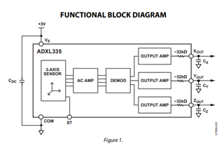
I am designing interface of single-ended source (ADXL354 accelerometer, with output impedance of 32kOhms) to delta sigma ADC model of ADS1288.
Since I do not have details of internal PGA differential amplifier of the ADS1288, may I use THS4551 or THS4501 models, assuming those are similar.
Thank you.
Hello Lkhagvahantsan,
I am switching this thread to the ADC team so they can support your questions on modeling the internals of the data converter.
If you end up needing a fully-differential amplifier I can assist you further. In general, you can use PGA and FDA models to simulate internal ADC blocks as long as you understand the specifications of the internal amplifiers within the ADC.
As I do not know what type of amplifier is internal to the ADS1288, I will have the precision ADC (PADC) team give their input here first.
Best,
Alec
Hi Lkhagvajantsan Damdinsuren,
As Mark mentioned in your other post (https://e2e.ti.com/support/data-converters-group/data-converters/f/data-converters-forum/1457609/ads1288-ads1288?tisearch=e2e-sitesearch&keymatch=%2520user%253A637038#), we do not have a model to share for the ADC input stage.
You should instead get the ADS1285EVM so you can perform any required testing and better understand the input stage characteristics.
-Bryan
Hello Alec Saebeler,
Thank you very much for your reply.
Yes I need the single-ended to fully differential amplfier stage, your assitantance is appreciated.
After that let me simulate internal ADC blocks.
The ADXL354 output has series resistance of 32kOhm, we will use external capcitor 27nF to set cutoff frequency to 200Hz, final ODR output data rate will be 125Hz for low noise seismic signals.
I insert here screenshot of ADXL335 MEMS acceleromter which is similar to target sensor ADXL354.
Best regards,
Lhagva
Hello Lkhagva,
Do you have a range for what the voltage of the output signals would be from ADXL335?
I can support designing a THS4551 front-end here and get you started before you consider ADC input structure.
Best,
Alec
Hello Alec,
Thank you for your reply.
ADXL354 has unipolar single ended output. The sensor has Output Full-Scale Range (FSR) of +-2g, Sensitivity is 400mV/g, so 2g will produce 800mV.
The 0 g bias output is nominally equal to V1P8ANA/2, where V1P8ANA is 1.8V and half of it makes 0.9V
Therefore output signal minimum will be 0.1V (represents -2g) and maximum will be 1.7V (represents +2g).
I imagine output of the THS4551 will be centered at 2.5V, gained about 1.8 times, which has approximate range of 1.06V to 3.94V. However I follow your recommendation on output of FDA..
Yes, please assist designing front-end circuit, after that we will decide ADC.
Best regards,
Lhagva
Hello Lhagva,
Great! Thank you for the explanation for the ADXL354, I knew you could explain it to me better than I could read it on the datasheet.
I will work on an FDA circuit for you and send it over once I have it simulated and understood to be good.
Best,
Alec
Hello Alec,
Thank you for your reply. I have thoroughly reviewed the datasheet.
Could you please recommend suitable evaluation boards along with your simulation results.
We plan to purchase ADS1285EVM-PDK Evaluation kit.
As Mark suggested, we have also reviewed the ADS131X0X ADC and consider it to be the best candidate for our requirements. However, for testing and evaluation stage we will proceed with ADS1285.
Best regards,
Lhagva
Hello Lhagva,
I would recommend the THS4551 EVMs, of which we have several THS4551 packages.
https://www.ti.com/product/THS4551#design-development
If you want a high input-impedance FDA, you can consider the THS4567. If you would need higher voltage supplies or increased input common mode range (or output voltage swing), you can consider the THS4561 and our newer THS2630.
Each of these FDAs has an EVM, though the THS2630 pairs with either the unpopulated DEM-FDA-xxx-EVM boards or the THS4130EVM.
Best,
Alec
Hello Alec,
Thank you very much for your recommendation.
Based on your simulation results we will choose FDA. Please confirm all of THS4551, THS4567 and THS4561 are also pair with either the unpopulated DEM-FDA-xxx-EVM boards or the THS4130EVM.
I imagine there will be an unity gain voltage follower after the ADXL354 output.
I wait for you to complete simulation to be good.
Best regards,
Lhagva
Hello Lhagva,
I will work on simulation. I will consider the need for a buffer between the ADXL354 output stage and the FDA circuit.
For EVMs, the D (SOIC), DGK (VSSOP), DGN (HVSSOP) are available on the DEM-FDA-xxx-EVM boards. These are unpopulated boards which support these three FDA packages. If you need to evaluate the RUN FDA package or would like to use the THS4551 / THS4567 EVMs, you can order those populated EVMs from those product pages.
As long as you confirm package pinout, the FDAs should function on an EVM which supports the FDA package of the IC.
Best,
Alec
Hello Lhagva,
I am still working on the circuit I promised to you; I want to check-in and see if you ordered any EVMs or have done any lab measurements?
Are any of the FDAs we discussed candidates for your system design?
Best,
Alec
Hello Alec,
Thank you for your work on the circuit.
We have not ordered yet the EVMs. Because we are also working on simulation for geophone amplifier circuit and once we complete simulation we will order boards. Since we require very low noise network for geophone, I am decided to use THS4551 and ADS1288. We will purchase THS4551DGKEVM, THS4130 EVM (replace THS4130 with THS4551 DGK), and ADS1285EVM-PDK (there are no EVM for ADS1288) accordingly.
As for MEMS ADXL354, the dynamic range is comparatively lower than geophone.
We will use ADS131E04 ADC (one channel for each ADXL354 output), but for FDA driver I consider THS4551, if you propose another we accept it (even FDA required or not?) and will purchase EVMs as required.
Regards,
Lhagva
Hello Lhagva,
Thank you for the update; I believe the THS4551 is a good choice for both systems.
If you more questions, please let me know.
Best,
Alec
Hello Alec
Thank you for your reply.
I have reviewed the datasheet again, and find that input voltage noise corner frequency is around 10kHz. But the signal we are measuring is seismic signals range of 0.1Hz to 100Hz. Do you have any suggestion for low noise FDA amplifier which has corner frequency less than 10Hz. If such a FDA does not exists we consider two op amp discrete circuit as well.
I am very much excited to see your simulation results.
Best regards,
Lhagva
Hello Lhagva,
Let me check the portfolio and discuss with my team on how I can help with a low(er) 1/f corner. Thank you for showcasing the lower-frequency signal requirements.
Best,
Alec
Hello Lhagva,
Do you have a target noise value for 0.1Hz to 100Hz? Are you asking for an extended curve showing more noise data or lower 1/f noise at low frequencies?
Please refer to the THS2630 noise curve for an example of a lower value voltage noise at low frequencies.
Best,
Alec
Hello Alec,
Thank you very much for your reply.
As for noise, the datasheet of the ADXL354 decribes noise density of 22.5 μg/√Hz, so for 0.1Hz to 100Hz band noise floor = noise density * sqrt(bandwidth)=22.5 * sqrt(100) = 225μg. The sensitivity is 800mV/g so noise floor RMS makes 800mV/g*225μg=180μV.
Yes, we are interested in lower 1/f noise at low frequencies.
Thank you for offereing low noise FDA THS2630, also I have been searching for and find out THP210 which has very low 1/f corner frequency.
Best regards,
Lhagva
Hello Lhagva,
Yes, the THS2630 would be an option for a high-speed FDA. THP210 is an option if you do not need the higher bandwidth and can safely operate under the specifications of the FDA.
What can also be done is this: you can put two low noise amplifiers (in gain) in front of the FDA; these low noise amplifiers can be selected for low 1/f noise. Their noise contribution will be greater than the second FDA stage.
Please let me know if you require additional design assistance here.
Best,
Alec
Hello Alec,
Thank you for your comment, I choose THP210 to safely operate under the specification.
I think we do not need additional two low noise amplifiers.
As I mentioned before we would like to purchase ADS1285EVM-PDK, DIYAMP-SOIC-EVM and OPA209AIDR, please tell me how we can place an order easily.
Best regards,
Lhagva
Hello Lhagva,
You can request samples of all three products at the following links:
https://www.ti.com/product/OPA209/part-details/OPA209AID?source=ooq
https://www.ti.com/tool/DIYAMP-EVM
https://www.ti.com/tool/ADS1285EVM-PDK?
You need to login with your TI account, scroll to 'Add sample to cart', and fill out your address information to check-out.
Best,
Alec
Hello Alec,
We have recieved samples, thank you for your support.
Do you have any question or clarification related to simulation.
Best regards,
Lhagva
Hello Lhagva,
I am glad you received samples.
If you still require simulation support for THP210, I can change-over the thread to the team who owns the THP210.
If you would still like simulation support for one of the THS45xx or THS2630 devices, I can still assist.
Best,
Alec
Hello Alec,
Yes, I am waiting for simulation support for THP210, please forward to THP210 team.
Below is summary of requirement:
The sensor is ADXL354 MEMS accelerometer for seismic application (single-ended output, with output impedance of 32kOhms).
We will use ADS131X04 for production, but will use ADS1285 for preliminary evaluation.
ADXL354 has unipolar single ended output. We will have 27nF capacitor at the output, 32kOhm and 27nF LPF will have 200Hz cutoff frequency.
The Nyquist frequency is 100Hz and ADC sampling rate is 200sps.
The sensor has Output Full-Scale Range (FSR) of +-2g, Sensitivity is 400mV/g, so 2g will produce 800mV.
The 0 g bias output is nominally equal to V1P8ANA/2, where V1P8ANA is 1.8V and half of it makes 0.9V.
Therefore output signal minimum will be 0.1V (represents -2g) and maximum will be 1.7V (represents +2g).
The analog accelerometer outputs of the ADXL354 are ratiometric to V1P8ANA. Therefore, digitize them carefully.
I imagine output of the THP210 will be shifted at 2.5V, gained about 1.8 times, which has approximate range of 1.06V to 3.94V. However I follow your recommendation on output of FDA.
As for noise, the datasheet of the ADXL354 decribes noise density of 22.5 μg/√Hz, so for 0.1Hz to 100Hz band noise floor = noise density * sqrt(bandwidth)=22.5 * sqrt(100) = 225μg. The sensitivity is 800mV/g so noise floor RMS makes 800mV/g*225μg=180μV.
Yes, the noise floor is comparatively high, however we are trying to get low 1/f noise.
Best regards,
Lhagva
Hello Lhagva,
I am adding the THP210 HVA team to this thread. Thank you for working with me and for trusting TI to help with your design.
Best,
Alec
Hi Lhagva,
Below is a preliminary circuit using the THP210 (FDA) and OPA2388 dual, zero-drift (Chopper amplifier) rail-to-rail input amplifier.
Comments:
- Since the sensor has a 32kOhm impedance, the sensor output needs to be buffered to drive the FDA.
- I chose the OPA2388 chopper amplifier, since chopper amplifiers virtually eliminate 1/f low frequency noise (choppers do not exhibit flicker noise)
- This amplifier circuit has very low noise at frequencies at the ~100Hz frequency range.
- Since the sensor has a 0.1V to 1.7V output centered at 0.9V, the FDA negative input is referred to 0.9V .
- The 0.9V is derived using a voltage divider, derived from V1P8ANA from the accelerometer.
- I assumed you plan to use a 2.5 reference for the ADS1285. Kindly let me know if this is not the case.
See Preliminary circuit below:
Questions:
1) Do you know if the V1P8ANA from the accelerometer is able to drive the 10k-10k voltage divider? If not, I will need to add another OPAx388 buffer prior the 10k-10k divider.
2) Since the measurements are ratiometric with respect to V1P8ANA, we will need a circuit to gain up this voltage and drive the ADS1285 reference inputs for better noise performance.
This can be accomplished using another OPAx388 circuit in dual-feedback configuration to drive the ADC reference inputs and bypass capacitor. Kindly let me know if using a ADC reference of 2.5V is acceptable; and if you want to proceed with this approach or you want to use a different ADC reference circuit on your side.
3) I assumed that the THP210, ADS1285 and OPA2388 are powered by a 5V unipolar supply, let me know if this is acceptable or if you have a different supply in mind.
I can provide detailed simulations (and if you wish, the ADC reference drive circuit), once I get your confirmation on the questions above.
Thank you and Kind Regards,
Luis Chioye
Hello Luis,
Thank you very much for your kind support and preliminary circuit.
Yes, I agree unity gain buffer is must be item.
Please see below my answers.
1. As for V1P8ANA output current, I have reviewed the datasheet of accelerometer again, but I can not find information about its ability to drive external load. Therefore I think we need another OPAx388 buffer for 10k-10k dividers 90uA. Can't we increase to 1M-1M divider so current is 0.9uA which might be negligible.
2. Yes ADC reference of 2.5V is acceptable, please proceed with this approach.
3. Yes, THP210, ADS1285 and OPA2388 are powered by unipolar 5V supply.
I would be happy if you provide me with detailed simulations, ADC reference drive circuit.
We are planning to test with ADS1285, please tell me a method how to calculate values R11, R12 and C11, C12 and C13.
As for production I am considering ADS1274 or ADS131X04 (even another appropriate ADC is accepted). I can confirm from datasheet of ADS1274 and ADS131X04 that we can choose lower fCLK for lower sampling rates, but the datasheet does not show noise measurement results for low sampling rates. Your suggestion for ADC selection is appreciated.
Best regards,
Lhagva
HI Lhagva,
I changed the front-end buffer amplifier from the OPAx388 to the OPAx187. The OPAx187 is also a chopper amplifier, with no flicker noise, but tends to be less sensitive to source impedance.
Chopper amplifiers offer very low offset drift, and no (1/f) flicker noise. This performance is achieved through the use of an internal calibration circuit that uses MOSFET switches to commutate the inputs. However, the chopper calibration technique generates small current transients within the amplifiers input bias current. These transients will flow through the amplifiers source impedance generating very small transient noise tones.
The OPAx187 is also a chopper amplifier, but it is less sensitive to source impedance, and works without any issues with source impedances up to 500kOhms. Since the application requires a 32kOhm +100pF low-pass filter at the accelerator output, and a voltage divider (we discussed on the post above, you may decide to adjust the voltage divider to higher impedance), Hence, I changed the buffer amplifier with the OPAx187 since this op-amp will be less sensitive to the source impedance, see table 5-1 below. The application note below provides a more detailed explanation on chopper amplifiers.
Optimizing Chopper Amplifier Accuracy
Attached are the OPAx187 + THP210 front-end Simulation results and simulation files.
- OPAx187 + THP210 Total output noise. The ADS1285 has a bandwidth (-3dB) of 0.413 x Fdata (due to the FIR digital filter). If the application requires a 200SPS sampling rate, the f(-3dB) BW is ~82.6Hz. The simulated total output noise of the OPAx187 + THP210 at 82.6Hz is 1.056uVRMS (or ~6.3uVpp using a crest factor of 6x)
Modified Circuit OPA2187+THP210:
Noise Simulation Result:
- Transient Simulation:
- Small-Signal BW:
OPAx187 + THP210 TINA-TI simulation file:
THP210_OPA2187_Front_End_noise_transient_AC.TSC
- Regarding the voltage divider, you can use a 1MOhm + 1MOhm voltage divider, (assuming the accelerometer/sensor can drive this high impedance). The total output noise of the circuit will increase to about 3uVRMS on the TINA simulation. The OPAx187 will see a source impedance of ~500kOhms which is still acceptable (per table 5-1 at the top of this post).
- For the ADC questions, it is probably best to consult with the ADC Applications team directly by submitting a query on the data converter forum; as they have up-to-date information of the ADC portfolio: https://e2e.ti.com/support/data-converters-group/
- I will certainly help with the Reference amplifier buffer simulations; I will look into using the OPAx187; I will update with the reference buffer simulation soon. I expect by Tuesday evening US time.
Thank you and Kind Regards,
Luis
Hello Luis,
Thank you for updating the circuit.
I found that we need to increase gain to 5x, even it saturates (peak acceleration recorded during the 2011 Tōhoku earthquake were around 2g).
Do I need separate reference chip for Vocm 2.5V for THP210 , or voltage divider will be sufficient as in current circuit.
I tried to simuate with PSpice for TI, please see attached results. As you can see AINP output noise (VONOISE, where input is Vin signal generator) is at level of 250nV. I am not sure I did correct simulation or not, your advice is appreciated. I am sorry I am not familiar with TINA-TI, I think I need to practice.
I am waiting for ADC reference circuit.
Best regards,
HI Lhaghva,
The OPAx388 and OPAx187 chopper amplifiers are difficult to compensate driving the large REFIN ADC bypass capacitor.
A good reference drive circuit is below, using the OPA210. The OPA210 is a bipolar input amplifier that offers very good DC accuracy and low 1/f noise. The op-amp can work at 5V unipolar supply, but the input common-mode requires a 1.5V headroom from the supplies, which is met in the circuit below.
The circuit uses the V1P8ANA from the accelerometer, and produces a 2.5V reference to drive the ADC.
The reference circuit is stable, and offers very low noise at 58nVRMS at 82.6Hz.
Noise Simulation of OPA210 reference drive:
Reference_drive_OPA210_Noise.TSC
Thanks,
Luis
HI Lhagva,
On PSPICE, to simulate and plot the total integrated noise, you need to use the function shown on the slides below.
See attached:
Thank you and Best Regards,
Luis
Hi Luis,
Thank you for your reference document.
I did noise simulation again. Please see attached results, the total RMS noise level is slightly higher than your results, however it is in nano volts level.
Unfortunately I can not increase gain to 5 by increasing feedback resistors R2, R4 of THP210. When I try to increase those resistors then convergence error occured, even I reduce tolerance it did not help.
Is it possible to change R2 and R4 to 5Kohm, or R1 and R3 to 600Ohm in real circuit?
Best regards,
Lhagva
Hello Luis,
Thank you for ADC reference circuit and simulation results.
Do I need R3 4.02ohm and R4 200mohm for real circuit, or are they used for simulation.
Please tell me what is the required tolerance for resistors around THP210.
I will create test board using the DIYAMP-SOIC-EVM, ADS1285EVM-PDK and ADXL354 evaluation board.
Best regards,
Lhagva
HI Lhaghva,
The circuit requires the R3 4.02-ohm resistor for stability. R4 (200mOhm) is optional, sometimes this resistor helps with transient response while driving the REF input on other more demanding un-buffered SAR ADC refence inputs. In this case, it is not required on the Delta-Sigma ADS1285 application. You could populate with a 0-ohm resistor or eliminate if you are concerned with area/cost. If you wish, you could consider adding an RC filter at the input, to filter any potential EMI or high-frequency noise, depending on the noise environment present in the application.
The tolerance and drift of the THP210 input and feedback resistors (R1, R2, R3, R4) needs to be selected depending on the gain error and gain temperature drift accuracy requirements in this application. These resistors will contribute to gain error and gain error drift. Also, the matching of the V1P8ANA voltage divider resistors will affect the accuracy 0.9V reference that tracks the V1P8ANA regulator. For the R-C-R filter at the output and the rest of the resistors, a 0.1% tolerance 25ppm/C is typically sufficient.
When using ceramic capacitors, choose C0G high-grade capacitors for the RC filters and feedback capacitors on the front-end signal chain. Among ceramic surface-mount capacitors, COG (NPO) ceramic capacitors provide the best capacitance precision and lowest distortion. The type of dielectric used in COG (NPO) ceramic capacitors provides the most stable electrical properties over voltage, frequency, and temperature changes.
You could estimate the initial gain error using Monte-Carlo analysis on PSPICE-for-TI. For example, on a different circuit with two separate gain stages, using 0.05% tolerance resistors at room temperature, will provide a typical (mean ±1-std deviation OR mean ±1 sigma) gain error of ~ ±0.05% (approx); and worst case (assuming ±3-sigma distribution) of ~0.15%.
Attached is a pdf file with a different Monte-Carlo analysis circuit example. The pdf file documents the basic procedure.
Monte-Carlo_Circuit_Example_PSPICE-for-TI.pdf
Thank you,
Kind Regards,
Luis Chioye
Hello Luis,
Thank you very much for your reply.
We added RC filter at the input.
Thank you for your design advice regarding the high grade component selection.
I tried Monte Carlo analysis but convergence problem arised and I could not complete simulation.
However we ordered components and will create test board soon.
Best regards,
Lhagva
Hi Lhagva,
I have not tried the Monte Carlo on this specific circuit. TheTHP210+OPA210 example on the pdf file worked without issue, but it is possible that the OPA187+THP210 combination could present issues converging.
On one case, when performing an AC Monte Carlo simulation on a different amplifier circuit, I modified some of the analysis parameters to help the circuit converge: All simulations convergence parameters were set to default, except for PTRANABSTOL (1e-5) and PTRANVNTOL(1e-4) under the “AC Analysis MonteCarlo” Simulation Profile, under “Options”, and “Bias Point”. These changes in parameters help speed up that circuit simulation.
On your circuit case, the simulation may be a transient simulation. Nevertheless, the PSPICE prompts on the “Output window” often provide suggestions for changes on the simulation parameters to improve, or speed up convergence.
Thank you and Best Regards,
Luis
Hello Luis,
We have X, Y, Z three axis of accelerometer.
Shall we use single 0.9V voltage source (U2, OPA187) for all channels, or we need separate op amps for each channel.
Best regards,
Lhagva
Hi Lhaghva,
If you decide to use a single op-amp, consider (if possible) using wide short traces on these connections with a symmetrical layout in attempt to reduce the trace connection resistance to a few 10s of milliohms and minimize errors on the 0.9V reference potential seen by the THP210. Each THP210 input could sink/source about ~700µA in simulation, depending of the input signal voltage level.
The OPAx187 can drive the 1kΩ input impedance of a single THP210. When a single buffer amp drives 3x THP210s, the amplifier will see a lower 1/3 input impedance load. Assuming this application is for 0.9V reference, a single may drive them as long this is a very low frequency 100s Hz signal.
Thanks,
Luis