This thread has been locked.

If you have a related question, please click the "Ask a related question" button in the top right corner. The newly created question will be automatically linked to this question.

AMC1301: How to build a simulation model for AMC1301?

Part Number: AMC1301
Other Parts Discussed in Thread: TINA-TI, ISO224, AMC3330, AMC1350

Tool/software:

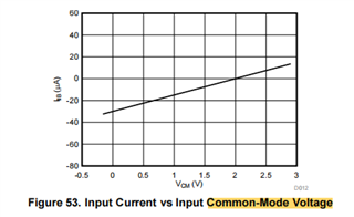
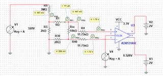
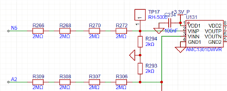
The attached diagram is the circuit diagram and simulation diagram of AMC1301, with an input DC voltage of 328V. Is the circuit on my simulation diagram correct? Also, what are the input bias voltage and bias current? 

Also, if no balance for input voltage offset, what are the impacts,  and what means to the balance input voltage offset ?

Also, why  R30=R3 ?

  • Hi Tom,

    I'm not quite sure what you mean, I see an ADxxx device on the simulation model. 

    You can find our TINA-TI and PSPICE for TI simulation models for the AMC1301 on the product page. 

    Please see this document for your other questions: https://www.ti.com/lit/an/sbaa350a/sbaa350a.pdf?ts=1736533312541

    This may help as well: https://www.ti.com/lit/eb/slyy234/slyy234.pdf

  • thanks !

     If connected in this way, how to calculate the input voltage?

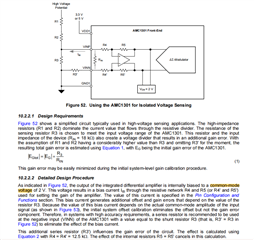
  •  Egot is the final gain, and according to the specifications, if R3 ' is connected, Egot should theoretically be equal to 0.

    In the formula, however, Egtot=Eg+R3/Rin。

    So, which of these two is Egot equal to?

  •  Also, how was the formula on page 4 derived?

  • If R3 and R3 'have been adjusted according to this formula,  is there no need to worry about the bias current?Any amount will not affect the

    gain error

  • Hi Tom,

    Please see the document I linked in my previous post. 

  • I have read it, but I cannot understand it. It states that as long as half of 22K (11K) is connected in parallel with the calibrated R3 to obtain the original value of R3, and R3 'is approximately equal to R3, correction can be achieved. Does this mean that as long as the aforementioned measures are taken, correction can be achieved regardless of the bias current?

  • If the intersection of R3 and R2 is C, initially Vc=Vs * R3/(R3+R1+R2). We now need to insert an active network containing resistor Rin and current I between point C and ground, ultimately achieving Vc=(1-R3/Rin) * Vs * R3/(R3+R1+R2)+R3 * I. That is, causing changes in both the original slope and intercept. May I ask what the structure of this network should be?

  • Hi Tom,

    Design of the front end can be complex, essentially the sensing resistance is in parallel with the differential input impedance, then the input bias current creates an offset. Both of these must be compensated for. 

    Please see the excel calculator for assistance with these calculations. 

    https://www.ti.com/tool/download/SBAR013/2.00.00.02

    Alternatively, have you considered using a device with higher input impedance and lower input bias current such as AMC3330, AMC1350, or ISO224? 

    All of these devices are more suitable for voltage sensing. The AMC3330 also features an integrated DC/DC converter which simplifies the design significantly. 

    Where are you planning on performing the sensing in your system? What type of application is it?

  • Thanks a lot ! 

    It would be even better if you could answer the question based on my premise。

    If the intersection of R3 and R2 is C, initially Vc=Vs * R3/(R3+R1+R2). We now need to insert an active network containing resistor Rin and current I between point C and ground, ultimately achieving Vc=(1-R3/Rin) * Vs * R3/(R3+R1+R2)+R3 * I. That is, causing changes in both the original slope and intercept. May I ask what the structure of this network should be?