Tool/software:
Hi,
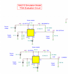
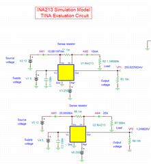
there are many reference designs or app notes where the terminology "minimum detectable current" or "minimum sensing current" has been used, for example SBAA243A. This is mostly related to the Vos of the used CSA and it is a little bit confusing for me.
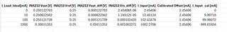
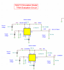
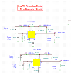
Let's consider a CSA where Vos is 500uV, Gain is 100V/V, bidirectional and we have Rsens 10mR. For this discussion the CMRR ane PSRR will not be considered. The minimum current that can be detected in this case is 50mA. Let's assume the Vref ist 2.5V. For the 0A load current the output of the CSA should be Vref +/-Vos*Gain = 2.55V or 2.45V.
If the load current is now 25mA, the output voltage will be:
a) Vref + Iload*R*Gain +/-Vos*Gain = 2.525V +/-0.05V = 2.575V or 2.475V
or
What would be the correct answer here?
If the load current is now 100mA, the output voltage will be:
c) Vref + Iload*R*Gain +/-Vos*Gain = 2.6V +/-0.05V = 2.65V or 2.55V
or
d) The output will see the load current only, because it is higher than Vos current, it means 2.6V?
What would be the correct answer in this case?
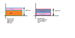
From my point of view the terminology "minimum detectable current" make sense for unipolar measurements where the output voltage swing limitation will limit the minimum input current, because the output will not change as long as the output voltage generated by input current is smaller than output low swing from the rail. It means the low voltage swing from the rail is going to "mask" the input current.
BR
Josko
a) and c) are correct. Even for unipolar measurements, the REF input (which many but not all CS amps have) allows moving the zero-current output voltage up. So even in this case, a negative offset voltage will make the output look like the result of a negative current.
Anyway, you are correct that the terminogy is inconsistent. The (constant) input offset voltage will result in a (constant) error at the output. I'd guess "minimum detectable current" simply means the minimum current for which you get a usable output even with the worst-case offset error.
Hi Josko,
The concept is actually very similar to swing limitations you alluded to. Basically the offset masks the input differential voltage if it is larger.
This train of thoughts assumes that we don’t look at the output before the differential input is applies. In other word, we had no idea what the offset is, and only look at the output once the input is applied.
Your calculations are correct for a specific part, and assumes the offset is known to be 500uV.
Regards
Guang
Hi Clemens, hi Guang,
thank you for your response and I am glad that my calculations are correct. Regarding the 500uV, I’ve just taken some number to simplify the math.
My idea is to build true zero unidirectional current measurements according to the attached block diagram. Therefore, I asked previous questions for better understanding of the concept. In this case the Vos calibration to 0A can be done any time during the relay is open, right?
I did DC analysis in TINA with INA123 reference circuit for 4 operating points and this should work well in my opinion. Do you have any suggestions or comments on block diagram or simulation results?
The concept is actually very similar to swing limitations you alluded to. Basically the offset masks the input differential voltage if it is larger.
My understanding of this is depicted on this picture.
If we go back again to SBAA243A where INA240A1 was used, the Vos of the INA240 is 25uV and for selected Rs =10mR, it gives min current of 2,5mA.
OPA320 has 150uV offset and THS4551 175uV, together they give us 320uV what equals 1,625mA referencing to the input. It gives together 4,125mA offset current, if my math is correct. I am curious why the min current is given as 50mA, if the total current error due to offset is around 4mA.
So, how we should define the MinCurrent in an uncalibrated system? Could it be a current where the error due to offset voltage is smaller than 10%?
Or if our system has the X [%] FSR gain error than the minimum detectable current should be the total Vos divided by X.
Edit: In the meanwhile I found this post here which gives more information about SBAA243A.
e2e.ti.com/.../ads8694-accuracy-reacheable-based-on-sbaa243
BR
Josko
Yes, you can calibrate out the offset error by forcing the current to zero.
In an uncalibrated system, you do not know the actual offset error, so you do not know the actual minimum current; you can only do worst-case estimates.
Hi Josko,
I think the calibration block diagram should work.
You're correct that min detectable current depends on individual application’s accuracy requirement. Therefore even with the same amplifier, the definition could be different for two projects.
Use INA240 as an example, Vos corresponds to 2.5mA. When measuring 2.5mA, we get a value that is anywhere between 0mA and 5mA (everything else is ideal). This corresponds to 100% error. But at 50mA, the error becomes a more manageable 5%.
Regards
Guang