This thread has been locked.

If you have a related question, please click the "Ask a related question" button in the top right corner. The newly created question will be automatically linked to this question.

OPA818DRGEVM: OPA818 Has excessive DC offset when used as a TIA

Part Number: OPA818DRGEVM
Other Parts Discussed in Thread: OPA818, OPA855

Hi this is a continuation of a ticket I submitted earlier when I reported that when using an OPA818 as a 7.5meg TIA. With no input conected I'm typically seeing about 30mV DC offset but when I test via a 7.5M resistor this DC offset increases to 130mV. I was told by TI apps that this was because with 7.5meg input resistor the OPA818 becomes an inverting opamp with noise gain of 2 which makes the part go unstable because noise gain needs to be at least 7. So I changed input resistor to 1meg so inverting gain is now 7.5V/V and noise gain is 8.5V/V which then satisfies OPA818 stability needs. Problem is this doesn't fix the issue ! With a 1meg input resistor effectively tieed between Vin+ and Vin- {still with the 7.5 meg feedback resistor and compensation capacitors) the output again jumps from 30mV to 130mV offset so it looks like the OPA818's aren't meeting their DC specifications.

From datasheet Vios max=1.8mV x8.5 = 15.3mV

input bias current max roughly = 25pA x 1meg = 25mV

input offset current = 25pA x1meg =25mV

So with everything at very worst case offset can't be much more than 65mV if part is within spec. Reality I'd expect to be much lower than this say 15.3mV + 5mV =20mV not 130mV.

Any thoughts ? best Steve

  • Hello Steve,

      Thank you for trying out the suggestion. 

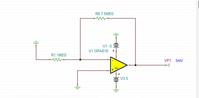
      Is the below the circuit configuration you have on the EVM:

      What is your compensation capacitors (do you have an input and feedback capacitor on the EVM?)

      Also, looking back at previous post, you mentioned that you had another EVM. Is it still showing the correct offset with the same exact configuration as your high offset voltage board when input is grounded?

    Thank you,
    Sima

  • Hi Sima circuit is correct, C feedback is <0.01pF and trimmable to tune out the effect of stray capacitance and tolerances. 7.5Meg resistors comprise three resistors in series to minimize capacitance. Shunt capacitance at the summing node needs to be in the range 20-80pF depending on where it is used. Oh yes the 1M Resitor is external to the board for test purposes only normally board is used as a TIA with input to the summing node. Thermal tab is isolated due to undocumented body diodes tying to substrate though I don't expect this effects issue at hand.

    So I've figured out the root cause of issue just tried looking with an active probe and spectrum analyzer and my hunch was right it's oscillating at 650MHz and the frequency/DC offset varies depending on shunt capacitance so we need to tame the OPA818. I know uncompensated broadband opamps can be tricky  but this one is intended as a TIA so am assuming it's doable. On your OPA818 datasheet you show bypass capacitors of 0.22uF and 0.01uF but these are going to be inductive above a few hundered MHz so may not be effective, do you have a better recommendation ? Alsp roblem with larger bypass capacitors is their inductance can resonate with smaller bypass causing resonant frequencies. Anyway will be interested to hear your recommendations best Steve

  • Hi Steve,

    Sima is out of office, but I can assist you with your question. If the device is unstable there could be a potential oscillation due to resonance between decoupling capacitors like you mentioned, but we have used these exact values for our fastest devices in there EVMs. OPA855 is a good example of the choice of decoupling on that much faster device. Does changing the values in your PCB change the oscillation frequency or the general behavior of the device?

    Best Regards,

    Ignacio

  • No unfortunately  changing values doesn't make any difference to the oscillations. Decoupling capacitors are all 0603 and close to power pins. The only thing I can think of is stray capacitance between inverting input and ground. Changing the OPA818 AC TIA input capacitive load does change the frequency of oscillations and DC offset. Best Steve

  • Hello Steve,

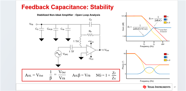
     Would you be able to try out smaller resistance values? With minimal feedback capacitance, this might be unstable due to the high resistor values interacting with the input capacitance of the device. 

      versus 

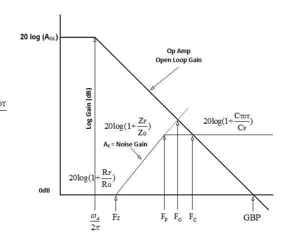
      In TIAs, you can go back to the high feedback resistor since your noise gain + stability is based on your input/feedback capacitance selection: 

        With an expected input capacitance of 20-80pF in a TIA configuration, you would then yes you would need around 0.01 to 0.02pF for stability at a 7.5Mohm gain resistor. This is difficult to achieve in practice if you need the higher bandwidth, calculators are saying it would be around 2MHz of closed-loop bandwidth.

    Thank you,

    Sima

  • Hi Sima, yes I agree but even the OPA818 package has a parasitic capacitance of approximately 0.1pF between output and vin- without factoring anything else so to get a reliable 1MHz bandwidth does require a lower transimpedance. However for this circuit we do need 7.5M transimpedance even if this means less bandwidth. 

    To eliminate layout issues we used a TI OPA818 eval board and modified it with 7.5M Rfb and our low capacitance network and with no input the offset was around 2.5mV as expected. Connecting our 7.5M input resistor/vsource offset goes up to 5mV still not too bad even though noise gain is x2. We then replaced 7.5M input resistor box with 1M and offset increased to 25mV implying offset is mostly due to Vios of the OpA818. We also tried different input load capacitances from zero to 84pf and nothing changed. We also monitored with a spectrum analyzer and active FET probe and saw no oscillations either on 500MHz scope or on 1GHz active probe.

    For our rev B board that is exhibiting the issue with Rfb = 7.5meg I first measured the DC offset with as 60mV with no input, I then increased the feedback capacitor and for Cf=0.4pF (plus strays on board) offset falls to 36mV, increasing to 0.7pF offset falls to 5mV so it looks like as the board is currently built we will either need higher Cf or lower Rf to eliminate the DC offset.

    Two questions for you would how the thermal pad is connected affect this at all? ie tied to 0V, tied to Vee or floating ? I ask because I know the thermal pad is connected to the substrate via body diodes and given oscillation is 500-700MHz any small inductance/capacitance will be critical.

    Second can you let me have part details for the 0.01uF and 0.22uF capacitors that you use without issue ? I ask because if you look at manufacturer's datasheets you will see that a 0.01uF 0603 NPO capacitor becomes self resonant above a few hundred MHz so neglecting any combo resonance with the 0.22uF capacitor the supply decoupling impedance is going to be a few ohms. Best Steve

  • Hello Steve,

      Thanks for the details! I apologize for the delay, I have just returned from business travel. Yes true for TIA you would be able to switch to an RF of 7.5MOhm resistor, but when configured as a standard VFB, then you would need to lower resistors since the lack of APD/PD internal capacitance + chosen feedback capacitance will have this amplifier be unstable. If you want to test out the high resistor value in a VFB configuration, you would need to manually add input capacitance of 20pF. But, it looks like you tried adding in this input capacitor and you saw no oscillations but there is still a high offset voltage? And this is on the TI EVM?

      What are the key differences from your Rev B board? I was assuming this was done on the TI EVM. If not, then yes if your Rev B is solved by increasing feedback capacitance, then it is probably an oscillation issue at very high frequencies. 

    For your two questions:

    1. For most of our devices, usually the thermal pad should be connected to VEE. But for this device the thermal pad is actually electrically isolated from the die substrate, and as you said, with ESD diodes down-bonded to the thermal pad. In that case, we connect it to ground on its own layer. But yes thinking about it, leaving it floating might sound better due to your reasoning, but since these ESD diodes are separate electrically to the die, it should not have any affect.

    2. Yes correct we usually recommend even configuring these as a pi filter or adding a series resistor. We almost always use X5R and X7R, NP0 are really good for filter and audio applications, but for decoupling capacitors for high speed signals you need to lower the inductance and this can be done by reducing the size of the capacitors. Also these threads from Kai and Michael have been very useful on layout and decoupling tips:
      1.  Question about proper decoupling 
      2.  OPA2350: op amp with thermal pad, best decoupling capacitor placement for Sallen Key LPF 
      3.  LMH6629: High-Speed Transimpedance Amplifier for Single-Photon Detection 

               And this thread on the capacitor choice reason:  TPA3251: Questions on power supplies and decoupling capacitors  

    Thank you!
    Sima

  • Hi Sima, the original board works pretty well for an input shunt capacitance range of 20-85pF. Where it oscillates is when you connect an input resistance to ground. Frequency changes but the DC offset gets worse as input resistance to ground is lowered. So 7.5M which you say would be unstable gives 13mV DC offset and a 1Meg input resistor which with a x8.5 noise gain should be stable still oscillates gives 25mV offset so Vios=2.94mV. Adding any shunt capacitance to ground to either of these if anything makes the offset worse. The newer board has worse offsets only real difference is more shunt input capacitance which based on the earlier version shouldn't be problematic. Moving onto your reference board as on our boards original spin input capacitance 20pF-85pF doesn't make much difference. Ti demo with 7.5M Rin noise gain=2 has only 5.6mV offset and no oscillation. Lowering this to 1Meg ie x8.5 noise gain offset increases to 21.7mV again has no oscillation and offset of 21.7mV so Vios is 2.55mV. Both of these numbers are very odd though because OPA818 datasheet claims typical Vios of 350uV and worst case over temperature 1.8mV and under these . Also note referred input offset is pretty constant whether noise gain is x2 or x8.5 and for the demo board at least no oscillations are visible at either noise gain. 

    Lowering transimpedance and adding capacitance may indeed be the only solution for the newer rev board unless we can figure out exactly what is causing higher offsets than original version. As I mentioned before the only real obvious difference is more capacitive load but as seen on the demo board this shouldn't make any difference.

    Thanks for answering my questions, glad to hear about the thermal pad and this corelates to measurements where pad is tied to Vee. We do currently have 10 Ohm series resistors feeding the opa818 rails with 0.22u + 0.01u(NPO) decouplers. I note that on the EVM both are just tied together with 1k BLM21 ferrite beads. I can certainly give this a try too because it will give better higher frequency decoupling.

    Best,

    Steve

  • Hello Steve,

    • "Original board works pretty well for an input shunt capacitance range of 20-85pF. 
      • That is good that TIA configuration works well!

    • "Where it oscillates is when you connect an input resistance to ground. Frequency changes but the DC offset gets worse as input resistance to ground is lowered. So 7.5M which you say would be unstable gives 13mV DC offset and a 1Meg input resistor which with a x8.5 noise gain should be stable still oscillates gives 25mV offset so Vios=2.94mV. Adding any shunt capacitance to ground to either of these if anything makes the offset worse."
      • I would say for this configuration it would be best to either use smaller value resistors but have the high gain (>=7V/V) or add the shunt capacitance to ground + an additional feedback capacitor. This combination of capacitors with the high valued resistors might work better. But, it would be easier to check configuration with smaller valued resistors. However, since it works already in TIA configuration this check might not be needed.

    • "The newer board has worse offsets only real difference is more shunt input capacitance which based on the earlier version shouldn't be problematic."
      • For this statement, I am guessing this is in TIA configuration. This might be due to any layout changes such as increase in trace length to the input of the amplifier (more inductance). 

    • "Moving onto your reference board as on our boards original spin input capacitance 20pF-85pF doesn't make much difference. Ti demo with 7.5M Rin noise gain=2 has only 5.6mV offset and no oscillation. Lowering this to 1Meg ie x8.5 noise gain offset increases to 21.7mV again has no oscillation and offset of 21.7mV so Vios is 2.55mV. Both of these numbers are very odd though because OPA818 datasheet claims typical Vios of 350uV and worst case over temperature 1.8mV and under these . Also note referred input offset is pretty constant whether noise gain is x2 or x8.5 and for the demo board at least no oscillations are visible at either noise gain. "
      • Would you be able to do a quick test with the default configuration of the datasheet as a control point? This would be with RF = 301Ohms and RG = 50Ohms and no additional input capacitance. This test if not needed if you are able to get your TIA board working, but suggesting if you want to check the reference board offset. That is strange that there are no oscillations, it might be filtered by equipment. Thanks for trying out all these tests!

    • "Lowering transimpedance and adding capacitance may indeed be the only solution for the newer rev board unless we can figure out exactly what is causing higher offsets than original version. As I mentioned before the only real obvious difference is more capacitive load but as seen on the demo board this shouldn't make any difference."
      • I went through this thread again, and I could not find this answer. I apologize if you already mentioned it, what was the differences between the original board and the newer rev board in terms of layout? 

    • "Thanks for answering my questions, glad to hear about the thermal pad and this corelates to measurements where pad is tied to Vee. We do currently have 10 Ohm series resistors feeding the opa818 rails with 0.22u + 0.01u(NPO) decouplers. I note that on the EVM both are just tied together with 1k BLM21 ferrite beads. I can certainly give this a try too because it will give better higher frequency decoupling."
      • No problem, I am glad it helped. The series damping resistors would help with resonance especially with longer traces = more inductance between supply to decoupling capacitor. The ferrite beads that is configured as a pi-filter on the EVMs helps with suppressing higher frequency noise as you mentioned. 

    Best Regards,

    Sima