This thread has been locked.

If you have a related question, please click the "Ask a related question" button in the top right corner. The newly created question will be automatically linked to this question.

THS4052 _Peak Detector

Other Parts Discussed in Thread: THS4052, OPA2132, OPA2277


Hello,

Please allow me to have a question  in addition to other post.

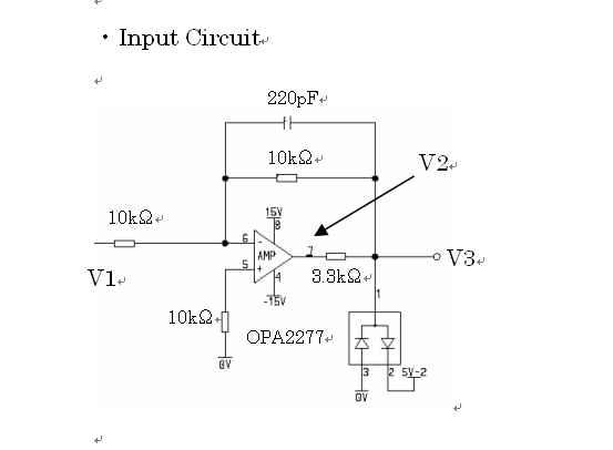
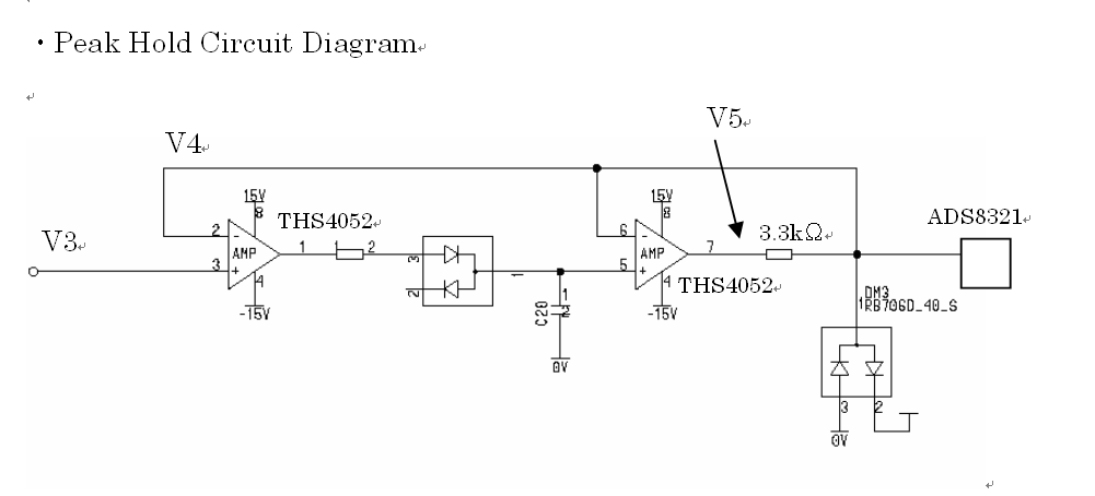
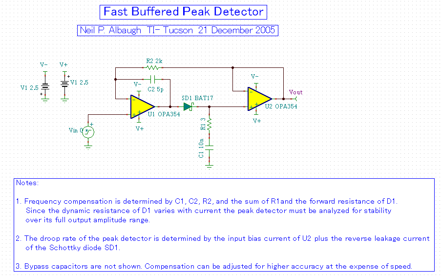
In case using THS4052 for peak detector, and also in case input voltage were large ( 5Vpp; 10KHz ),

the large bias current = 3.3mA into IN- and from IN+ were ovserved un their PCB ( pre-production )...

Cusomter and I also don't know the mecanism/root cause about his.

If customer changed the Opamp to uPC812C and OPA2132 , such a phenomenon did not  observed. 

We wnat to know the root cause..

Here I attached the question and wave form  as .jpg file again.

I am sorry to bother you again, but please advise.


  • Hello Kanji-san,

    This is really strange behavior. I still need some data-points to dig into this further:

    1. You mention that V1_Hi = 5V and V1_Lo = 0V. However from the figure it looks like V1_Hi = 0V and V1_Lo = -5V? Can you please calrify.

    2. In order to dig deeper, I would like to understand the clamp voltage on each of the diodes shown and any other dc bias voltages. Can you please send me a high resolution picture of bith circuits (OPA2277 and THS4052)

    3. When I compare V4 and V5, the signals are inverted. When V5 starts going down, V4 starts going up. This is truly bizarre. Can you remove the clamp on the output of the 2nd THS4052 and check results as well. (May need to remove the ADC to prevent damage).

    4. Can you make sure that when probing with a scope, attach a 1K series resistance to the scope probe tip to isolate its capacitance from the opamp terminals and prevent any further interaction.

    We are looking to get into the old design database as well to further understand the internal architecture of the device.

    -Samir

  •  

    Dear Samir-san


    Thank you for your responce!!


    1. You mention that V1_Hi = 5V and V1_Lo = 0V. However from the figure it looks like
    V1_Hi = 0V and V1_Lo = -5V? Can you please calrify.

    ==>

    Yes You are correct...

    2. In order to dig deeper, I would like to understand the clamp voltage on each of the
    diodes shown and any other dc bias voltages.
    Can you please send me a high resolution picture of bith circuits (OPA2277 and THS4052)

    ==>

    Thank you for your comment, I attach the schematic again

    3. When I compare V4 and V5, the signals are inverted.
    When V5 starts going down, V4 starts going up.
    This is truly bizarre. Can you remove the clamp on the output of the 2nd THS4052 and
    check results as well. (May need to remove the ADC to prevent damage).

    ==>

    I will ask customer, and I will infrom you later

    4. Can you make sure that when probing with a scope, attach a 1K series resistance to
    the scope  probe tip to isolate its capacitance from the opamp terminals and prevent any
    further interaction.

    ==>

    Thank you for your commnet

    I will check customer's test method.

    Is that mean " Scope== Probe= 1Kohm( in series) == OP amp terminal " using ative probe ?


     Best Regards


    Best Regards


  • Hello Kanji-san,

    Thanks for the circuit, it helped me see some of the details a lot better in order to analyze the circuit.

    I have been working with the designers to get to the database for the device, however the server has been moved a couple of times and now we cant seem to find the original design. I dont have any EVMs with me currently for testing so I have placed an order for some EVMs. It should be here next week and I can try things on the bench then.

    I do think there are stacked diodes on the THS4052 and this is what is causing the circuit the behave the way it does. One thought I have to possibly fix the circuit is to limit the current that can be provided to the clamping diodes internal to the THS4052. However we have to do this without causing any voltage drop at Pin V4 (Pin 7 of the 2nd THS4052). I think the best way to do this is to insert a resistor (say 1k-10k) between Pin 6 of the 2nd THS4052 and Pin2 of the 1st THS4052. We may have to play around with this value of resistance

    In addition to this I think we will have to eliminate the 3.3KOhm resistor at pin 7 of the THS4052 as well. The reason for this is that the presence of that resistor can cause the 2nd amplifier of the THS4052 to go open loop when it is providing the current back to the 1st opamp; we want to prevent this from happening and removing the 3.3k will help enable this.

    Please let me know if the customer can try this out.

    -Samir

  • Dear Samir sanThank you for your reply. I will chech to customer.
  •  

    Hello


    Thank you for your answer!!


    According to cstomer, removing the clamp diodes after the 2nd OP amp( THS4052 )

    did not fix the problem....


    (1)

    Also , according to customer, the 3.3Kohm resistor at the 2nd OP amp is used in order to drive ADC properly,

    so customer says it can not be removed..... customer says they don't know the meaning of 'Open loop' below .

    Would you please let us know the meaning of ' Open Loop'? if available.


    ~~Your answer~~


    that resistor can cause the 2nd amplifier of the THS4052 to

    go open loop when it is providing the current back to the 1st opamp;

    ~~~~~

    (2)

    Anyway, I found the sample design (TINA  desiged by Mr Neil P Albough /BB ) , attached..

    Would you please  let us know how to select the value of  R2 ( 2K ohm ) and C2 (5p )  ?

    I could not find any app note for this.


    P/S

    Customer ( and I ) think if  there were stacked ( 4V ) back to back diode inside of THS4052,

    customer and I think this phenomenon is make sense....


    Thank you and I am sorry to bother you again..

    Best Regards


  • Hello Kanji-san,

     I ran some tests in the lab yesterday and confirmed that there are 4 series diode clamps between the inputs of the THS4052 amplifier.

    Attached is a power point document showing what I mean by amplifier going open loop. I  think we will need to remove the 3.3KOhm resistor from the circuit. Keeping it in there will cause the 2nd amplifier to also go open loop because: "current has to flow through the ESD diodes of the 1st amplifier -> this means there is now a volatge drop across the 3.3KOhm resistor which will prevent the 2nd opamp from being in a buffer configuration".

    With regards to choosing the value of R2, I would say that you want to make R2 large enough to account for the voltage drop and current through the ESD of the 1st THS4052 amplifier. So say you have an input signal going from +13V to -13V. The peak detector action will cause the output of the 2nd amplifier to stay close to +13V (peak). Lets say that V3 is now around -13V. Lets also say you want the ESD clamp diodes to barely turn-on, then the voltage across the 4 diodes is around 2.8V. Unfortunately, the THS4052 does not have a max. input current spec, so for now lets play it safe and assume 2mA max. Then {13V- (-13V+2.8V)}/2mA = 11.6k. I will leave C2 =1pF to 5pF. Note that all this assumes the 3.3K is not present...otherwise as mentioned earlier the 2nd amplifier does not act like a unity gain buffer.

    Peakdetector.pptx

    -Samir

  • Dear Samir san


    Thank you for your detail desctiption and answer, I appreciate for you

    Thanks and with my best regards