This thread has been locked.

If you have a related question, please click the "Ask a related question" button in the top right corner. The newly created question will be automatically linked to this question.

OPA2317 overstress

Other Parts Discussed in Thread: OPA317, OPA2317

Hello team , 

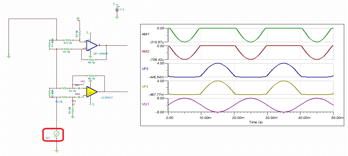
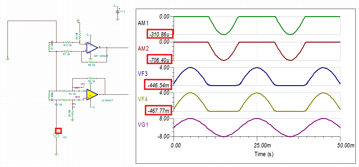
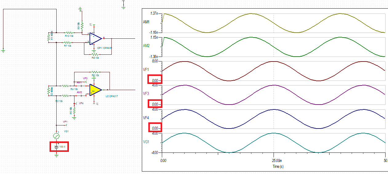
some of my customers are using the circuit attached below as a bi directional current sense 

Inverter_current_monitor.TSCBasically each op amp gives voltage across the rsense in half cycle 

outputs of these op amps go to the uC where they are read

in my conversation with BU , it was pointed out that this architecture would violate the Absolute maximum ratings of the input pins of the op amp

However due to the high value resistance connected at the input the current flowing through the internal diodes is limited 

Can you please help me understand more about this architecture , and if we are indeed violating the input absolute max specs can we modify it slightly to make it acceptable 

Thank you 

  • Shreenidhi,

    The specified OPA317 input common-mode voltage range is 100mV beyong the rails, which in your single supply application, with Vs=5V, means from -0.1V to 5.1V -  see below.

    Let me first bring it to your attention that your circuit might be confusing and thus needs to be corrected to make sense - the violation of the input common-mode range occurs in case of negative input signal but because you flipped VG1 input signal generator it apears to happen on positive input - see below.

    After correcting the polarity of the input signal generator, the clamping of the VF3 and VF4 input common-mode voltage occurs as expected for negaive VG1 - see below.

    Because OPA317 includes reverse-bias ESD protection diodes from each input terminal to each rail, apllying negative input signal turns them on and results in input clamping around 450mV below the ground as well as hundreds of uA input current flowing thru the diodes - see above. 

    The Absolute Maximum input voltage of 300mV beyond the rail is shown in the table below; applying -4V at the input terminals (Vcm=8V/2) would cause a damage if the current was not limited to less than 10mA.


    However, because of the 10k resistors, the input current is limited to less than 1mA and the op amp will not be damaged.

    One way to bring the circuit into compliance with the specified input common-mode range is to offset the signal by +4V - see below.

    For more details on EOS, please review the TI Precision Labs material under following link:

  • Thank you marek
    Your reply does answer my question
    We are safe as the 10k ohm is restricting the flow of current into the input pin of the ic


    Basically the sine wave generator shown in the schematic is nothing but the 50Hz sine wave ( India = 50Hz , usa = 60Hz) being generated on the primary side of the inverter/UPS . this will be stepped up using a step up transformer to make the 220V/110V sine wave to power up the grid connected loads

    the output of the OPA2317 shall be connected to two different pins of a Uc ,
    the uc will read take the output of only one opa2317 valid during each half cycle ( either during positive half cycle or during negative half cycle )

    Thus we can have bidrectional current sensing without using negative supply or reference ic