This thread has been locked.

If you have a related question, please click the "Ask a related question" button in the top right corner. The newly created question will be automatically linked to this question.

OPA1632: Need to reduce the offset at output side

Part Number: OPA1632
Other Parts Discussed in Thread: TINA-TI

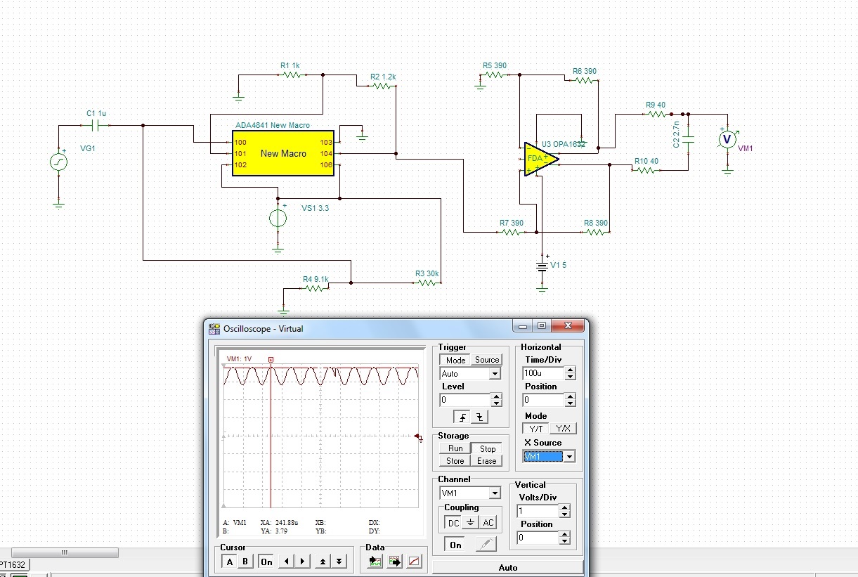
Referring to the attached simulation, I am using OPA1632 following the output from ADA4841. The output from ADA4841 has output of 2.2Vpp and offset of 1.78V, I am connecting the output to OPA1632 which has Unity gain just to make output from Single ended to Differential. I have given 2.2 Vpp and im getting 1 V on each side so that is fine but i have a requirement that maximum peak on both outputs should not be more than 2.8V but my output at R9 has reached 3.79 as shown in simualtion. Please suggest how can i adjust my output to be within 2.8V peak.

  • Hi Kiran,

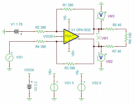
    The primary reason you see the OPA1632 output at R9 to reach 3.79V peak is due to the DC offset between the OPA1632 inputs at R7 (1.78V)  and R5 (GND). This can be corrected by applying similar DC levels at both the inputs or making the DC level at R5 same as R7 (or 1.78V). This way, there is no input DC offset and both the OPA1632 outputs are centered around the default output common mode voltage (or 2.5V in your schematic).  

    Since you have mentioned that the maximum output peak is limited to 2.8V, the output common mode DC voltage needs to be shifted down to 2.2V. This can be done by tying the OPA1632 Vocm pin to 2.2V, which results in the  maximum swing of 0.5V peak to occur around this 2.2V or giving 2.7V as the maximum peak voltage.

    I have attached the TINA-TI schematic with the corrections if you want to take a look at it.

    Best Regards,

    Rohit

    OPA1632_UnityGain.TSC