This thread has been locked.

If you have a related question, please click the "Ask a related question" button in the top right corner. The newly created question will be automatically linked to this question.

INA114: INA114 failure problems

Part Number: INA114

We have had some internal failures (14 in last 6months)of TI INA114BP with Lot Codes: (49Z7INW, 42Z7IMW, 48Z788W). I am inquiring if anyone using this part has had any history of complaints for any failures of these lot codes for this part. .Primary cause of failure (per Lab Specialty) excessive heat >150 C, (possibly during wire bonding) that has caused the wire bonds to lift. Please inform us of any info you may have on this problem.]

  • 26 views and 6 hours after posting and still no one at TI can reply to this?
  • Micheal,

    Looking into lot history of any potential failures of INA114. Will let you know what I'll uncover.

  • i have pulled some information from the TI website, Document # "SNOA069C Device Marking Conventions", but am still confused:
    the chip i have in front of me at the moment is marked with "49Z71MW":
    going by the decoding convention that i have from the website, this chip was made in 2014, September, Wafer Lot Code Z71M and was manufactured in Japan ("W"), however, the distributor that we buy these from states that the country of origin is Malaysia, not Japan.
    we also have some of these chips that are marked with "2CZ05CW", that also confuses the decoding, unless the 2nd digit for the month is supposed to be for "March", whereas, other chips have a "3" for March.
    This all seems very inconsistent.
  • Micheal,
    It turns out that INA114 device has a die coat so if the device is in a high temperature environment, there is a possibility there could be voiding in the inter-metallic which could cause the bond to lift. In die-coat products there is a higher susceptibility to open wires due to Kirkendall voiding than with other devices. However, we reviewed those specific LTCs and the assembly lots they were derived from and haven’t had any returns on those lots.

    TI has verified that our products can meet the terms of the datasheet in respect to maximum operating temperature but I would like to ask following questions:

    - What are the nominal storage conditions for the units in your inventory?
    - Are the units run through any temperature processing prior to reflow which is used to filter out early-life failures?
    - How many reflow passes does your PCB receive?
    - Could you please send a schematic for review? We’ve seen cases where a high current sink through a particular pad results in very high localized heating which can drive the Kirkendall voiding reaction.
  • Jay,

    The wafer fabrication may have been in Japan but '49Z71MW' code is an assembly lot and ‘W’ stands for Malaysia and not Japan.  Thus your distributor is correct that the country of origin is Malaysia.

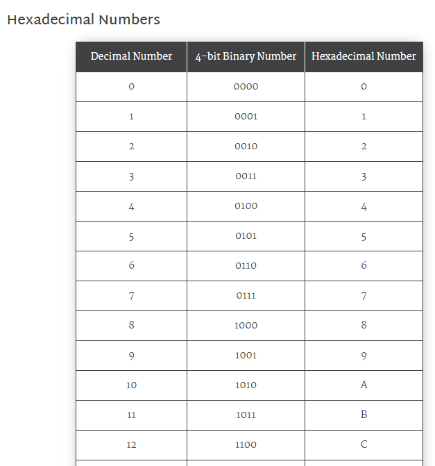
    As far as you second question goes regarding '2CZ05CW' code, C does NOT stand for March.  Since it may be difficult to encode twelve months in a single digit, the Device Marking Convention uses Hexadecimal numbering scheme; thus ‘C’ stands for December – see table below.

  • Hi Marek,

    Here are answers to your questions - some info is from Note (the CM in China) , other info (schematic) is from PCI:

    1.       What are the nominal conditions for the units in your inventory?

    a.       Raw materials (PCB, electrical parts, metals parts) & work in process (WIP) in the manufacturing floor  -    i.      Under controlled environment – 18-28 deg. Celsius / 35-65 % for humidity

    b.       Solder paste – 0-7 deg. Celcius

    c.       Finish Goods – normal room temperature storage at Ware house (this is an open area) – staging goods in this area is not long when it reaches this area we schedule shipment as soon as the units are ready to go (estimate within 7 days, less or additional more days depending on situations)

    2.       Are the units run through any temperature processing prior to reflow which is use to filter out early- life failures

    a.       No (not unless otherwise to be specified and we can add this process as necessary)

    3.       How many reflow process does your PCB receives

    a.       None. PCBA is a through hole assembly. And INA114BP parts are through hole package. Run through wavesolder only.

    b. Wavesolder process specs:

    Solder Time = 2.15s ~2.75s, Conveyor Belt speed = 100cm/min, Solder peak temperature = 236.84 degree F.

    4.       Could you please send a schematic for review?

    Schematic section for INA114BP:

  • Hi Marek,
    I can't seem to paste in schematic.
    Can you send me your email address to my email address so that I can send you the schematic for INA114BP use.
    Thanks
  • Micheal,

    You need to use Rich Formatting option and press one of the buttons at the top of the reply window to Insert Media or Insert File.