This thread has been locked.

If you have a related question, please click the "Ask a related question" button in the top right corner. The newly created question will be automatically linked to this question.

OPA847: Voltage Noise Peaking in Transimpedance Amplifier (TIA) - why does the addition of a feedback capacitor cause voltage noise peaking?

Part Number: OPA847
Other Parts Discussed in Thread: OPA820, LMH6629, OPA657

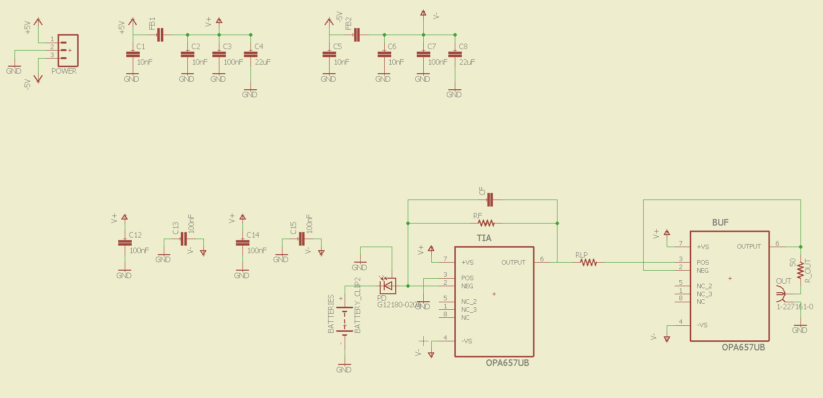
I am working on a low noise transimpedance amplifier (TIA) for the detection of weak optical signals. The aim is to achieve a 10MHz bandwidth with a white voltage noise floor of 10-20nV/rtHz. I am using the FGA21 photodiode and the OPA847 Op-Amp with a 10kohm feedback resistor operating in photoconductive mode.

Key specifications include:

  • Gain banwidth product: GBW = 3.9GHz
  • Input voltage noise: e_n = 0.85nV/rtHz
  • Input current noise: i_n = 2.5pA/rtHz
  • photodiode capacitance: C_d = 100pF @ 3V bias

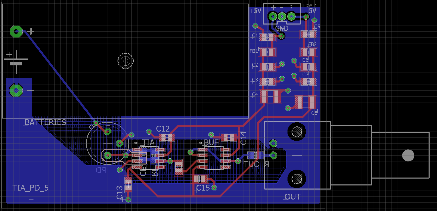
The PCB design followed many of the suggested layout techniques (minimising track length, passing feedback components under the op-amp, isolating sensitive tracks from the ground plane etc.). Additionally, the voltage supply was heavily filtered using decoupling capacitors and the OPA820 Op-Amp was used to buffer the output.

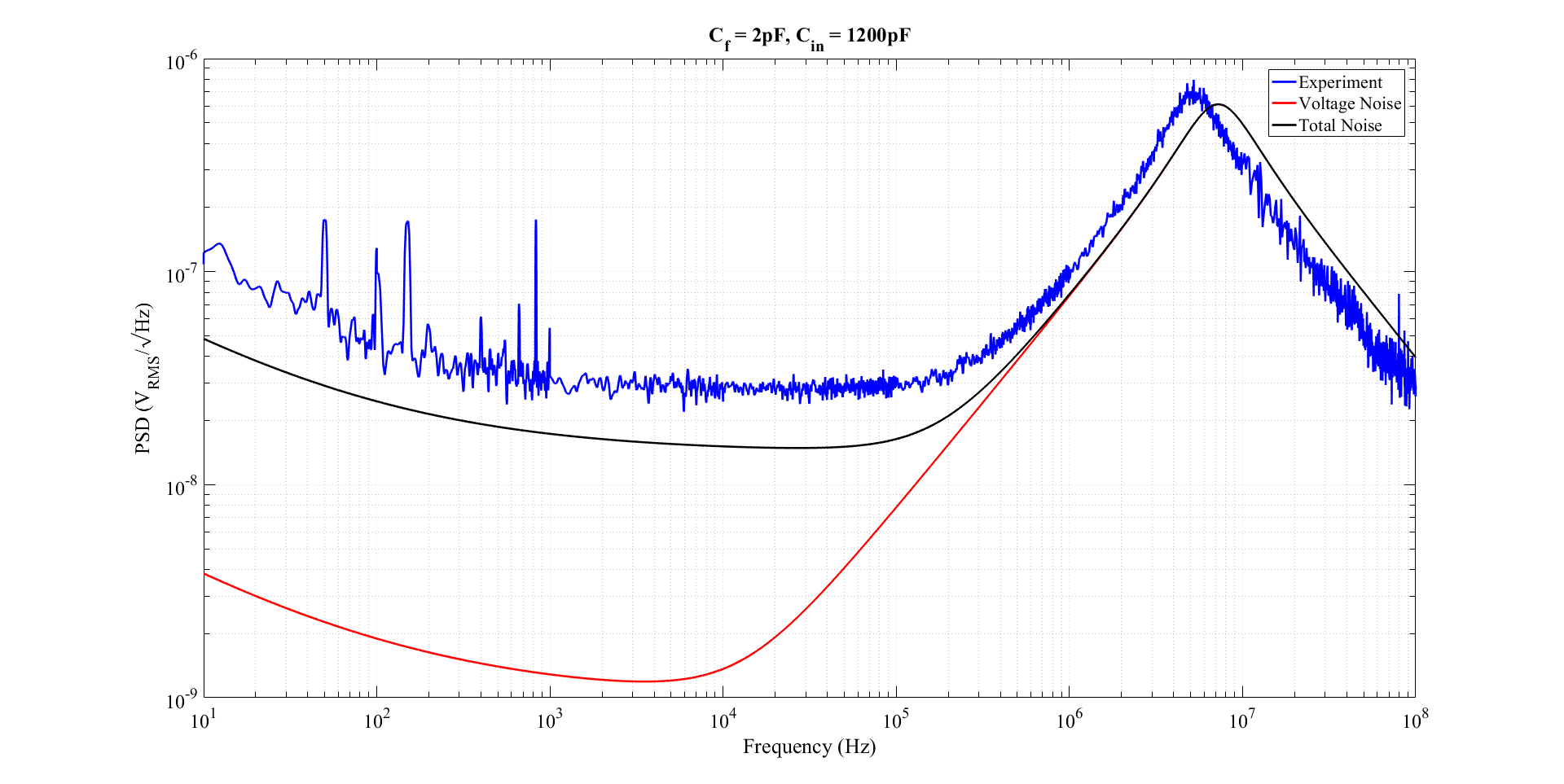
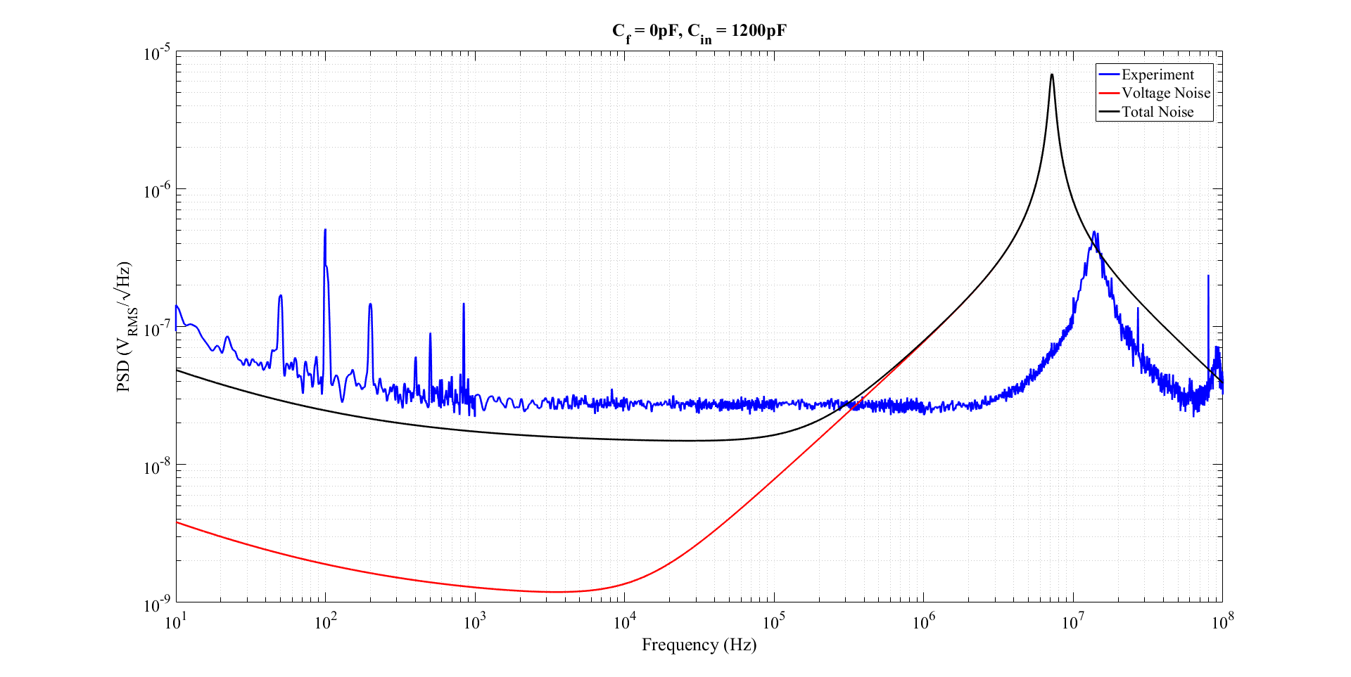
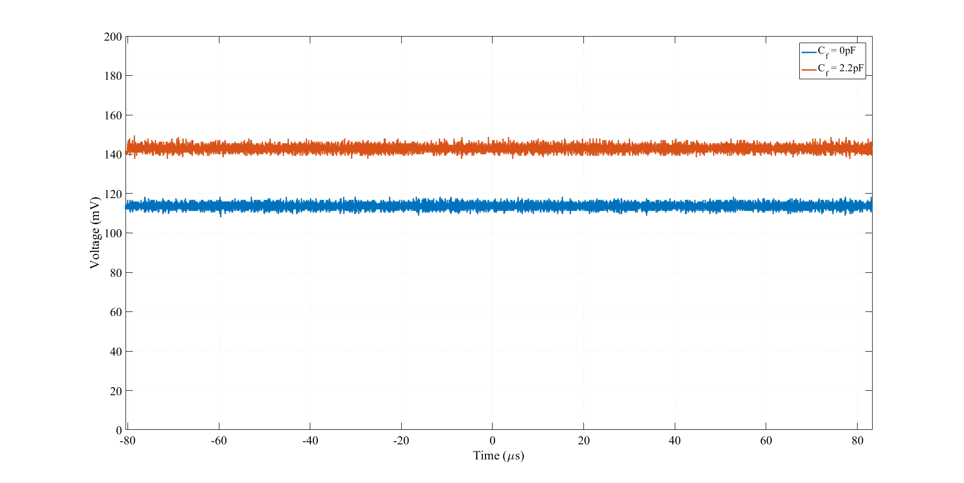
Two noise spectra were taken, one where the feedback capacitance was left open and one where it was set to 1.5pF:

TIA Noise

The dashed lines represent the corresponding theoretical noise curves. Clearly the capacitor causes the noise peaking to broaden and shift in frequency, this contradicts theory which suggests that a feedback capacitor dampens the transimpedance gain and reduces high frequency noise.

So I am wondering if anyone else has come across this issue before or can understand how the addition of a single capacitor causes a large disparity between theory and experiment?

  • Hello Joshua, Great question. To answer this you need to familiarize yourself with the concept of noise gain. I will use figure 3 of the OPA847 datasheet to illustrate.

    Figure 3 has three main passive components:

    Feedback resistor Rf, Feedback capacitor Cf and a photodiode capacitor Cin which in this case is 1pF and can be thought of as a 1pF capacitor to GND at the amplifiers inverting pin. One needs to add the OPA847s input capacitance (common-mode =2pF and differential =1.7pF) to the total input capacitance. The OPA847s input capacitance can be found on page 3 of the datasheet under "INPUT". So the total input capacitance, Cin = 1pF + 2pF + 1.7pF = 4.7pF.

    Now to analyze noise gain take the amplifiers input noise (0.85nV/rtHz) and apply that noise source at the non-inverting terminal of the amplifier and find the transfer function to the amplifiers output. You can ignore all the resistor components at the noninverting terminal as they don't affect the voltage noise or noise gain.

    So at low frequencies Cin and Cf can be considered "OPEN" so the amplifier is in unity noise gain.

    At a frequency equal to approximately 1/(2*pi()*Cin*Rf) there is a "zero" in the noise gain response which will cause NG to start increasing. This is the rise you see in the noise gain. The fact that the noise gain in reality starts increasing earlier tells me that the input capacitance in your real circuit is larger. It is also possible that the model does not have the right value of input capacitance.

    The noise gain will increase until 1/(2*pi()*Rf*Cf) at which point there is a pole, so it will hit a maximum and the amplifiers bandwidth will cause the noise to start going down. At high frequencies the noise gain amplification is given by 1+(Cin/Cf). So if you have no Cf that is a divide by zero so the noise will just start increasing to infinity. In reality you do have some feedback capacitance from parasitics (100-200fF) and so that limits the noise.

    However what is happening in your case is that the noise gain pole is too small and is beyond the amplifiers Aol, so the amplifier bandwidth starts to reduce the noise again.

    So smaller Cf will actually increase the noise gain and a Cf too small can also cause potential oscillations. The OPA847 is stable only in gains of close to 20V/V and above.

    Check out these documents to learn more on how to stabilize TIAs:

    e2e.ti.com/.../what-you-need-to-know-about-transimpedance-amplifiers-part-1

    e2e.ti.com/.../what-you-need-to-know-about-transimpedance-amplifiers-part-2

    www.ti.com/.../sboa122.pdf

    There is a calculator included as a link in the blog posts to guide you on how to calculate Cf. I would recommend using the LMH6629 instead of the OPA847. If I use the calculator with the following parameters, it tells me you can achieve a bandwidth of around 25 MHz and need a feedback capacitance of around 0.9pF.

    Calculator I
    Opamp Gain Bandwidth Product (GBP) 4000.00 MHz
    Feedback Resistance (RF) 10.00 kOhm
    Input Capacitance (CIN) 103.70 pF
    Closed-loop TIA Bandwidth (f-3dB) 24.78 MHz
    Feedback Capacitance (CF) 0.909 pF

    -Samir

  • Hello Samir,

    Thank you so much for your in-depth response, it is incredibly helpful.

    The input capacitance being much larger then expected is not something I had considered. I am relatively new to circuit design so it is possible that there is extra capacitance at the input (although I have tried to follow many of the design techniques for TIA's suggested online). With this in mind I have changed the input capacitance in my model to try and fit the theoretical noise curves to experimental data:

    Here is the noise curve for R_f = 10kohm and C_f = 2pF. I have increased the input capacitance to 1200pF as this produced the best fit with the experimental data. I have only plotted the voltage noise contribution to total noise as that is the dominating term at higher frequencies (although the total noise does consist of current, shot and Johnson noise components). As you said, due to the higher input capacitance the noise gain increases much earlier and we see a much better fit to experiment.

    However, if I keep the input capacitance the same and consider the case of C_f = 0pF I observe the following:

    Again due to the higher input capacitance the voltage noise starts increasing at a lower frequency, however this time it is not consistent with experimental values as our experiment suggests with no feedback capacitor the roll up in noise begins at a much higher frequency.

    So it appears that by increasing the input capacitance significantly the theoretical noise better fits experiment only in the case where a feedback capacitor is present. In my understanding I have considered the feedback and input stages separately, however the data suggests that a feedback capacitor is causing drastic changes to the input stage. Is this something you are aware of or have come across before?

    For reference please find attached the schematic and board layout of this circuit, if you have any questions about my design choices I would be happy to expand further.

    Regards

    Joshua

  • Hi Samir,

    Just another quick (and I think rather interesting) update. I replaced the OPA847 with the OPA657 and observed the following:

    Clearly now we see a much better agreement with theory (I believe the elevated white floor in the blue data is the floor of the spectrum analyser). My first thought is that the 847 is a bipolar input whilst the 657 is a FET input device. Would you know why a bipolar input device would cause such issues?

    Thanks again

    Josh

  • Hello Joshua,

    Are you using a physical capacitor or are you using a photodiode when measuring the noise? Your layout looks good and I cannot see how there could be an extra 200pF of capacitance.

    Does the Iq of the OPA847 change when going between no Cf and Cf = 2pF? I checked the phase margin of the amplifier and with Cf = 0 (or very low) your phase margin is under 20 degrees which suggests instability. I wonder if that is changing the characteristic of the amplifier. Can you compare Cf = 2pF and Cf = 4pF and see what happens.

    When comparing BJT vs FET inputs the 1st thing to consider is the current noise. You can ignore current noise in a FET input amp. I checked the current noise of the OPA847...3.5pA/rtHz * 10kOhm = 35nV/rtHz. That is where you see your noise floor. Also, I do know that the current noise of the OPA847 starts to increase above 10 MHz. I wonder if the low phase margin in the case of Cf = 0 is making the amplifier act up and change something in its profile.

    Do you have the ability to inject a signal into the non-inverting pin? If you did we would be able to check the actual noise gain of the amplifier.

    -Samir
  • Hello Samir,

    In this test I am using a physical capacitor, previous measurements I have used a photodiode whilst measuring noise and the behaviour observed with the OPA847 is consistent in both cases. It might be worth changing the feedback capacitor to a higher value to see what happens, my current choice of 2pF allows a reasonable phase margin whilst preserving the required bandwidth, however, for our understanding it might be worth sacrificing bandwidth by increasing Cf further.

    Although the current noise is lower in the FET input device I do not believe we are dominated by current noise in the OPA847 at high frequency, it appears to me that when Cf is increased from 0pF to 2pF it is voltage noise which is increasing as the slopes match (both go as ~f).

    I do not have the ability to inject a signal into the non-inverting pin without breaking tracks in the circuit. Is it possible to inject a low voltage test signal into the inverting pin or does this raise other problems?

    Thank you for all your help

    Josh

  • Hello Josh,

      Unfortunately it wouldn't do much good to inject into the inverting side. Injecting into the noninverting side would give us a noise gain measurement.

    -Samir

  • Hi Samir,

    I will look at the possibility of taking a noise gain measurement on my current circuit.

    Another question I have regarding the OPA847, in figure 3 of the spec sheet they give an example of a TIA with the non-inverting terminal grounded through a 12kohm resistor to "reduce the contribution of input bias current errors (for total output offset voltage) to the offset current times the feedback resistor". In my current circuit the non-inverting terminal is routed straight to ground, do you think it is a possibility that input bias current errors are somehow causing an increase in noise at the MHz region? It could explain why I do not see this issue in the FET input op-amp as bias currents are negligible.

    Josh
  • Hello Josh,

      The matching resistor on the noninverting terminal is only to match the offsets on either side and will not in itself affect the bias current. However, if the amplifier is unstable that could cause the Ib to vary. Can you please check the output offset voltage of the OPA847 with Cf = 2pF and open.

    -Samir

  • Hi Samir,

    Here is the time trace for Cf = 0pF and Cf - 2.2pF:

    It appears that, as you were suggesting Ib is changing with a changing Cf. It should be noted that with Cf = 0pF the output offset is very stable (as it is for Cf = 2.2pF).

    Thanks

    Josh

  • Josh, Can you please try 4-8pF and see if there is further change?

    Also do you by any chance have a loop antenna and a spectrum analyzer so you can make noninvasive measurements to see if there are any high frequency oscillations?

    -Samir

  • Hi Samir,

    I do have access to a high frequency (up to GHz) spectrum analyzer, although I do not have the data recorded I have seen quite bright spectral lines at ~750MHz. If necessary I can record this data and send it to you.

    Thanks

    Josh

  • Joshua, Do you see the spectral peaks for both feedback caps? Don't bother capturing the data. I am just trying to make sense of what may be happening here. I am a little behind on work right now so don't have the time to verify all this myself in the lab.

    -Samir

  • Hi Samir,

    I have recorded high frequency (up to 1GHz) data for the case where Cf = 0pF and have increased the feedback capacitance as you suggested to Cf = 5.6pF, this is shown below:

    So by increasing the feedback capacitor it seems to dampen the 5MHz peaking but increase the white floor significantly. We also this time see the bright spectral lines between 100MHz and 1GHz. It appears that adding a feedback capacitor causes the lines to brighten and side-bands become more prominent.

    Josh

  • Hi Josh, there is something wrong with the 5.6pF curve. The higher noise even at low frequencies (1kHz-100kHz) is not expected. Did you maintain the same feedback resistor or did you increase the resistor? If the resistor is the same size then I think the device is possibly oscillating which is increasing the amplifier noise. Was the power consumption with 5.6pF Cf the same as with 2.2 pF?