This thread has been locked.

If you have a related question, please click the "Ask a related question" button in the top right corner. The newly created question will be automatically linked to this question.

INA2128: Output Frequency Response

Part Number: INA2128

Hello,

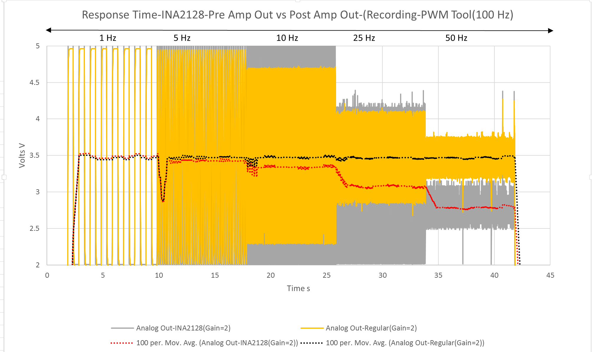
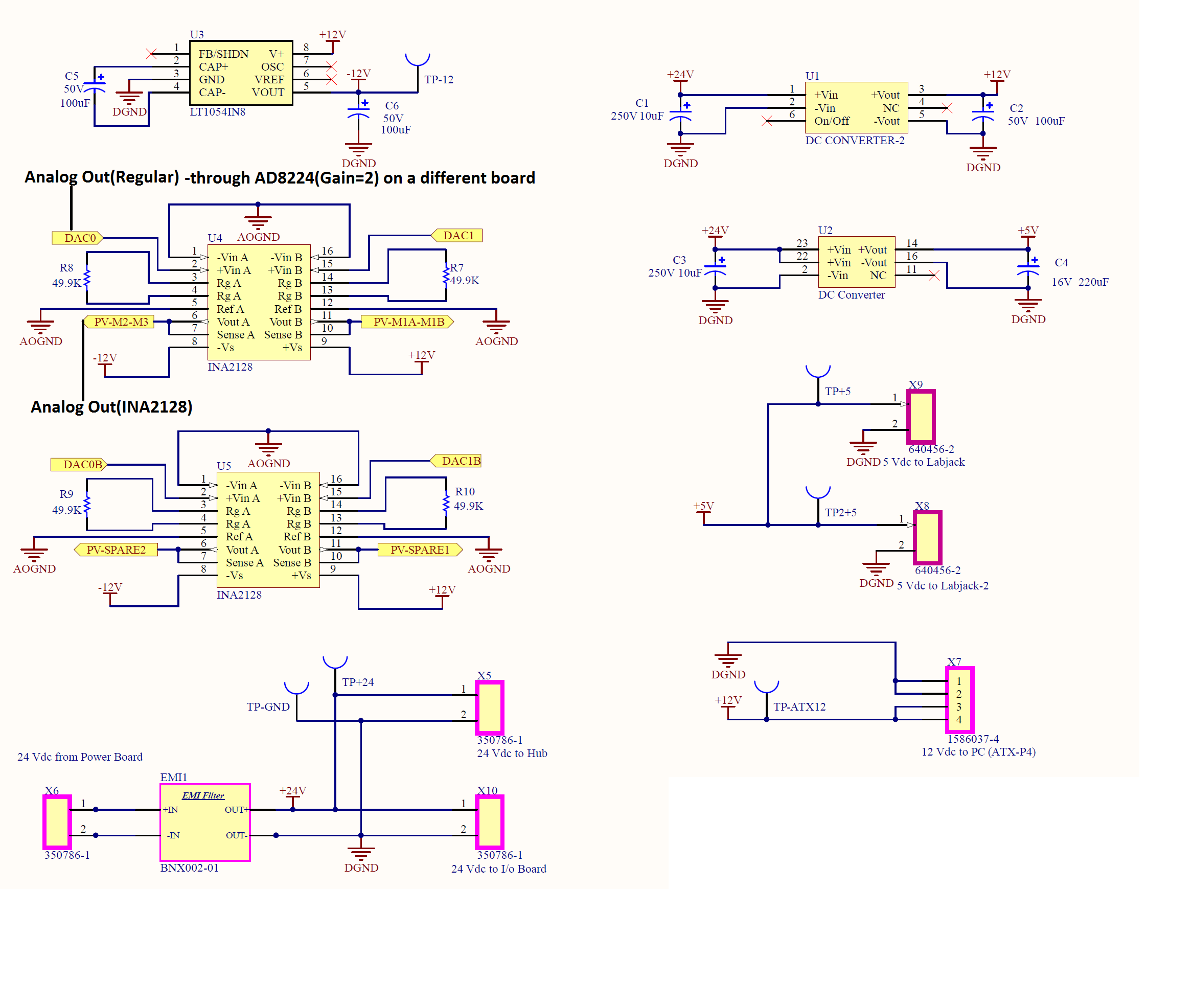
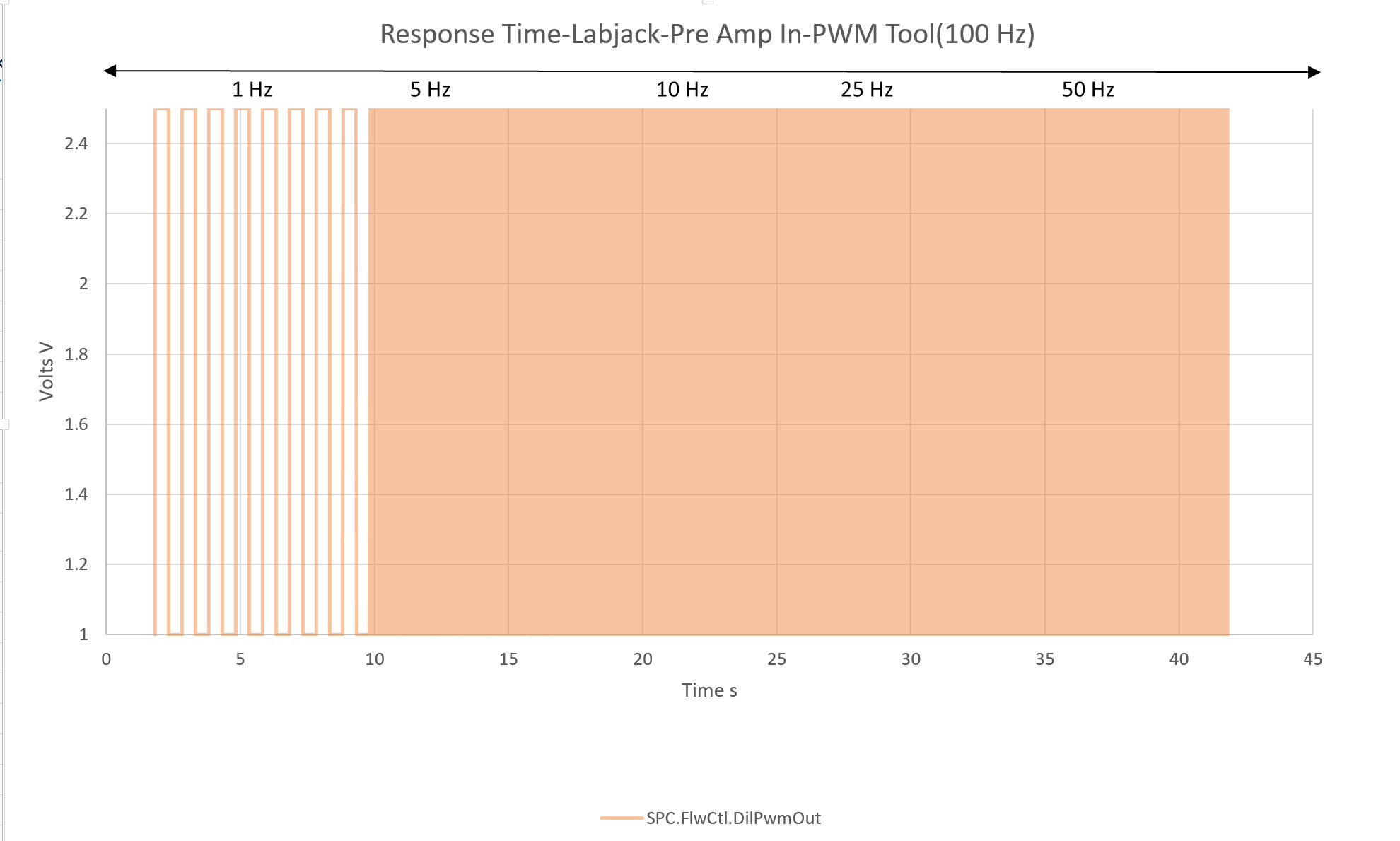
I'm using INA2128 Instrumentation amplifier for Analog Out amplification(Gain=2). I'm testing the amplifier circuit for frequency response and response time using a recording tool. Below is the graph for comparison between Analog Out before and after the Amplifier circuit. It seems like the Amplifier out is not averaging at higher frequencies for some reason and there is an attenuation issue, is this because of some filtration or aliasing? I can provide the schematics as needed.

Please help me understand the issue and what would be a fix for this kind of behavior.

Thanks,
Naveen.

  • Hi Naveen,

    What is the purpose behind this measurement technique? The conventional method for measuring gain vs. frequency is to apply an analog sine wave of constant amplitude level to the input, and measure the output level as the frequency is swept over a specified range.

    You are testing the INA2128 with a square wave that may have fast edges. Moving up in frequency the slew rate of the INA2128 might become an issue. If the slew rate is not symmetrical for the rising and falling edges that could affect the average value.

    What is meant by Analog Out-Regular? Go ahead and send us your circuit schematic. Show the supply voltages, input signal characteristics and the output load. That might give us a better idea of what you are doing.

    Regards, Thomas
    Precision Amplifiers Applications Engineering
  •  Hello Thomas,

    Thanks for the quick response.

    We're trying to charecterize a new single board computer(SBC) that we're planning to incorporate in our application and we're doing various preformance tests to compare it to the previous computer we had in our application.The new single board computer Analog outs are 0-5 Volts. This lead us to use INA2128 Amplifier with Gain=2 for Analog Outs.

    Analog Out(regular) is a bit misleading, sorry for the misscommunication. We've an AD8224 Instrumentation amplifier on a different circuit board. We're feeding- Analog Out directly from the SBC to the AD8224 Amplifier with Gain=2, as you can see in the graph, that's the expected behavior at higher frequencies (averaging out at 3.5 V).

    Analog Out(INA2128) is the output from the INA2128 Amplifier which is fed with an Analog Out from the SBC directly.So, it's basically comparing two different Amplifier Outs at different frequencies.

    Input signal is a system write for the Analog Out. It's just a square wave with changing frequencies after regular intervals with an amplitude of 1.5 V.(below)

    As you can see in the earlier graph, the clear difference in the Amplifier outs(also repeatable) is prompting concerns.

    Attached is the schematic for the circuit board with INA2128. This board serves as an interface board between the SBC I/O system and different circuits boards down the line in our application.

    Regards,
    Naveen.

  • Hello Naveen,

    Thank you for the additonal information. This is certainly a different kind of testing than we normally do so we don't have any information about what to expect from the INA2128 when it is subjected to it.

    I do have a some questions:

    1) Does the INA2128 have any power supply bypass capacitors at its V+ and V- pins? The minimum supply pin bypass is a 100 nF from the pin, directly to ground. The addition of a 1 uF to 10 uF in parallel with the 100 nF would be preferable.

    2) What is the input impedance of the instrument attached to an INA2128 output?

    3) The ideal PWM square wave output appears to have an voltage range from +1 V, to +2.5 V. Is that correct?

    4) Have you observed the supply voltage at the V+ and V- pins with a DSO as you exercize the INA2128 at the different PWM frequencies?

    5) Do you know what the rising and falling edge rate (dv/dt) is for the input square wave at each of the different PWM frequencies?

    Regards, Thomas
    Precision Amplifiers Applications Engineering
  • Hello Thomas,

    1) I don't have any capacitors directly connected between the power supply pins and ground. There are 100uF capacitors at the output of the power supply itself(both positive and negative) as shown in the circuit. Would that make a difference in the output of the Amplifier?

    2)For testing purposes, the output of the Amplifier is directly fed to an Analog Input of our I/O System(Labjack T7), if you're asking for that, it's
    1 GΩ.

    3)Yes. that's correct. The output from the amplifiers is twice the amplitude as shown in the first graph because of the Gain setting.

    4) We didn't pay much attention to the power supply since the AD8224 Amplifier's output was as expected. But, just to make sure, I can repeat the test and post the results.

    5)If you're asking for rise time and fall time of the Input signal(system write), that's 10 ms, that's the system delay.
  • Hello Naveen,

    Sorry your inquiry got lost amongst the many we receive. Regarding your answers:

    1) I don't have any capacitors directly connected between the power supply pins and ground. There are 100uF capacitors at the output of the power supply itself(both positive and negative) as shown in the circuit. Would that make a difference in the output of the Amplifier?

    Providing proper supply bypassing is a standard engineering practice with analog circuits. The recommended 100 nF capactor bypass capacitors should be connected directly from the power supply pins to ground, with the shortest possible electrical path. The capacitors serve as charge reservior for the amplifier, and provides filtering of higher frequency noise. It also decouples the INA2128 power supply line from other amplifiers connected to the same power supply lines by providing a low ac impedance to ground.

    2) For testing purposes, the output of the Amplifier is directly fed to an Analog Input of our I/O System(Labjack T7), if you're asking for that, it's 1 GΩ.

    Okay, so there isn't any resistive loading issue. Keep in mind if that is a long cable that could represent a sizeable capacitance to the INA2128 outputs. A capacitive load could alter the settling characteristics of the third amplifier stage inside each INA2128.

    3) Yes. that's correct. The output from the amplifiers is twice the amplitude as shown in the first graph because of the Gain setting.

    okay

    4) We didn't pay much attention to the power supply since the AD8224 Amplifier's output was as expected. But, just to make sure, I can repeat the test and post the results.

    Did you ever have a chance to observe the supply pin behaviors with a DSO at the different PWM frequencies?

    5) If you're asking for rise time and fall time of the Input signal(system write), that's 10 ms, that's the system delay.

    Okay, that is slow and probably isn't an factor.

    Regards, Thomas
    Precision Amplifiers Applications Engineering