This thread has been locked.

If you have a related question, please click the "Ask a related question" button in the top right corner. The newly created question will be automatically linked to this question.

OPA3692: OPA3692 --- Two Input One Output Video Amplifier/Buffer - Disable line problem

Part Number: OPA3692
Other Parts Discussed in Thread: TINA-TI

OPA3692 Problem

Setup:

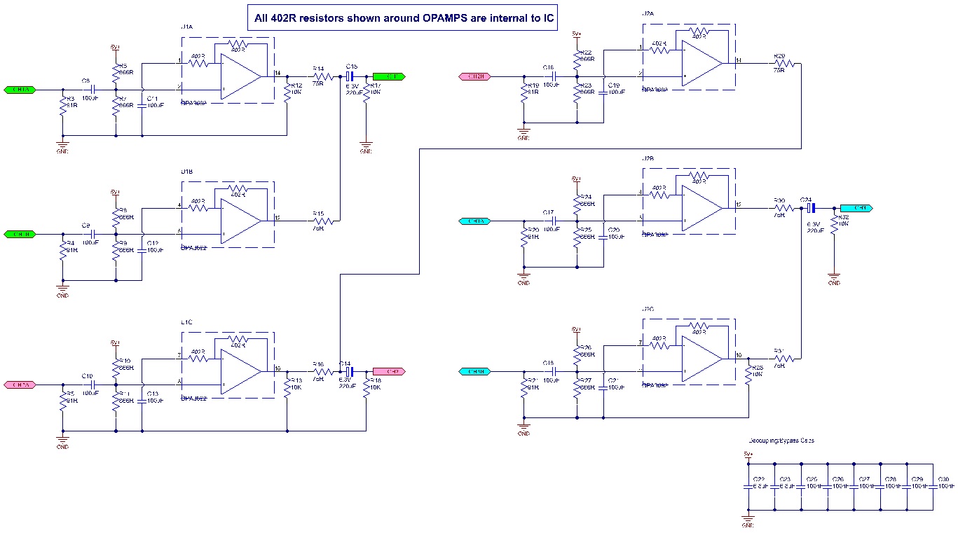
Two (2) Opamp ICs OPA3692 are used with 6 OPAMPs in total (as each OPA3692 has 3 OPAMPS). The 6 OPAMPs are divided into 3 groups. Each pair is exactly same as below so, only testing only first pair (See Figure1).

The pair takes input from two different video sources at CH1A & CH1B (in Figure-1) and channels only one input to the output (CH1 in Figure-1) depending upon the DISABLE LINE (Ignore U2D as it belong to second OPA3692 IC – see Figure2) (The other pairs also take inputs from different sources and send the signal to their own respective output channels)

The drive circuit for DISABLE Line is also shown in Figure-3. The Inputs SOL1 & SOL2 are driven from 24V control lines from a different board. (However, this circuit was also tested by pulling DOWN the DISABLE lines of Amplifiers by putting short circuit across C31 & C32 in Figure-3 to ensure that DISABLE Line of OPA3692 is pulled down to 0V – This had no effect on the results)

OPAMP has 6.8uF & 100nF Bypass Caps on Supply Rail (5V) and not shown in the pictures below


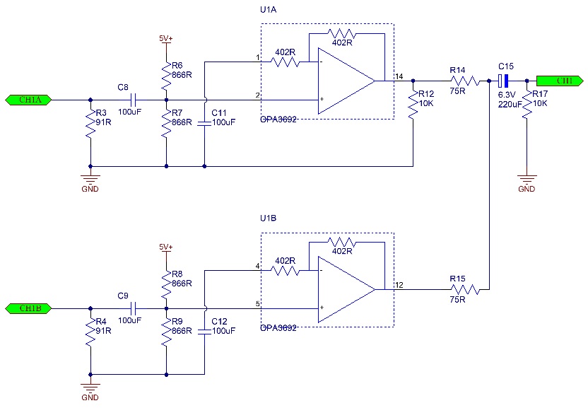
Figure-1: One pair of two input – one output video amp/buffer


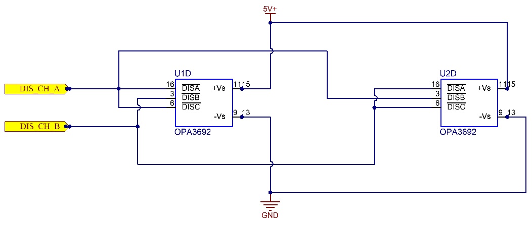
Figure-2: Disable lines & Power Supply blocks for OPA3692 – ignore U2D as it belongs to 2nd OPA3692 IC

Figure-3: DISABLE Lines drive circuitry – Also tried to disable by putting short circuit across C31 & C32


Results:

With Disable Line on both amplifier switched OFF (pulled DOWN):

Ch-A: Input Video Signal (Blue) (@ CH1A – above schematic) (Grey scale bars from a video tester)

Ch-B: Output Video Signal (Red) (@CH1 – above schematic) (Only oscilloscope connected at output with No Load)

(No Video Signal Applied on CH1B input)


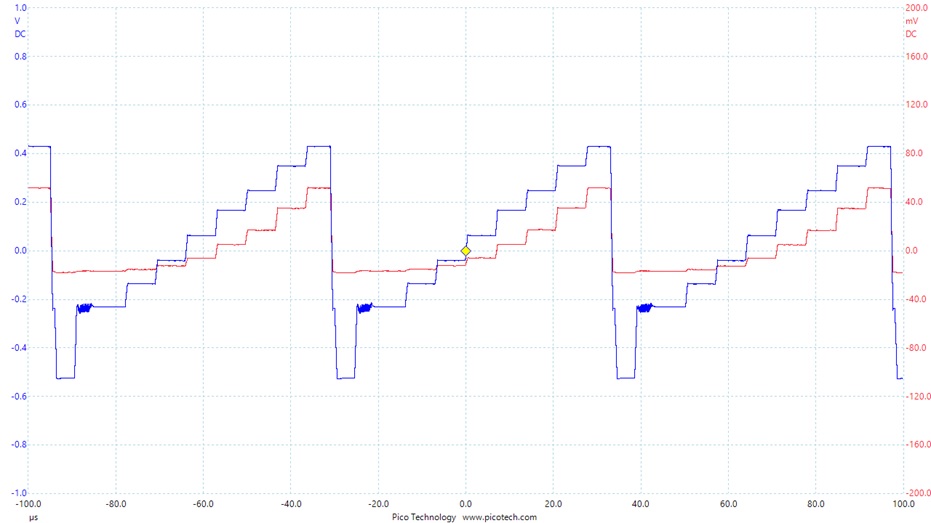
Figure-4: DIS Line pulled LOW for U1A & U1B – but there is considerable video signal (RED) at the output that appears as dim lines when TV is connected at the output (TV was not connected when this trace was taken)

!!!This is problematic issue!!! As it was expected to be similar to Figure-6 Negligible signal at output – see below)


 ------------------------------------------------------------------------------------------------------------------------------


With Disable Line on amplifier U1A switched ON (apprx 3.6V) & on U1B switched OFF (pulled LOW)

Ch-A: Input Video Signal (Blue) (@ CH1A – above schematic) (Grey scale bars from a video tester)

Ch-B: Output Video Signal (Red) (@CH1 – above schematic) (Only oscilloscope connected at output with No Load)

(No Video Signal Applied on CH1B input)


Figure-5: U1A enabled and output is almost same as input (as expected) (Similar traces were observed if Video Input is applied at CH1B with U1A disabled & U1B enabled)


 ------------------------------------------------------------------------------------------------------ 


With Disable Line on amplifier U1A switched OFF (pulled LOW) & on U1B switched ON (apprx 3.6V)

Ch-A: Input Video Signal (Blue) (@ CH1A – above schematic) (Grey scale bars from a video tester)

Ch-B: Output Video Signal (Red) (@CH1 – above schematic) (Only oscilloscope connected at output with No Load)

(No Video Signal Applied on CH1B input)


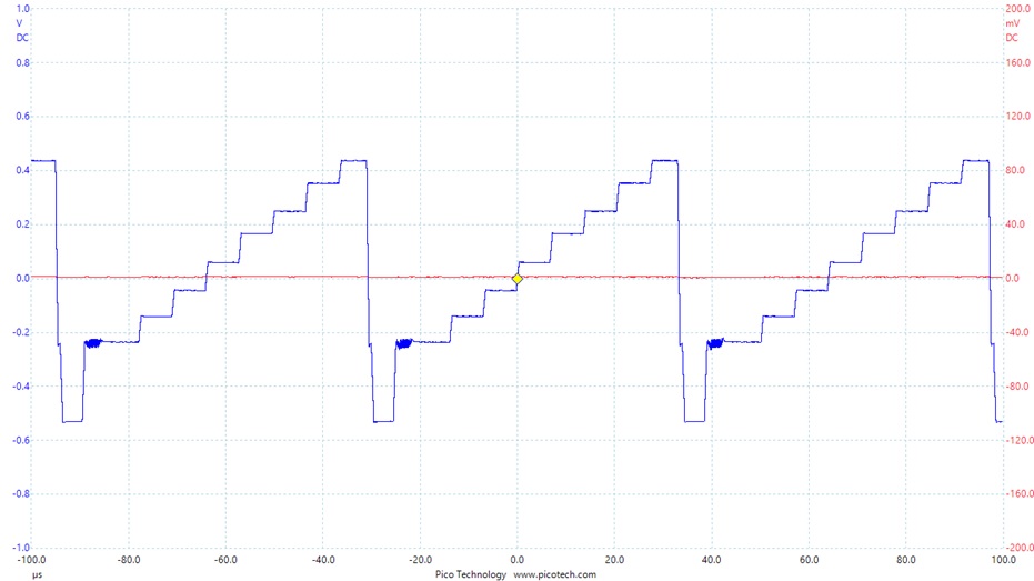
Figure-6: U1A is disabled but U1B is enabled (with No Video Signal at U1B’s input). Output is flat apprx 0V as expected (No dimmed lines on TV if connected at the output)


 -----------------------------------------------------------------------------------------------


Problem:

As it could be seen in Figure-5 that with both amplifiers disabled (either using the drive circuitry of Figure-3 OR by putting a short circuit across C31 & C32), there is small signal at the output which manifests itself on TV screen as dimmed lines. I was expecting it to behave like it is shown in Figure-6 but that requires Enabling at least one amplifier which is not how it is intended to be used in field. The amplifier specs in datasheet show that:

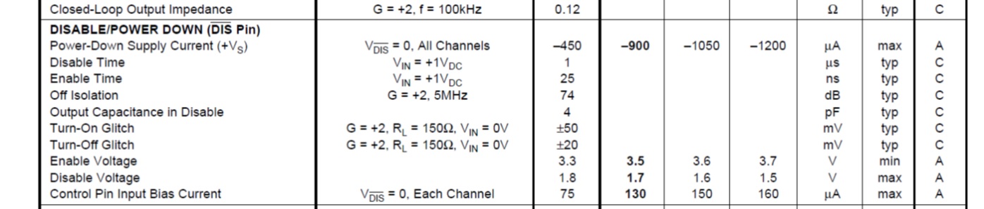
Figure-7: Off Isolation Specs from Datasheet


I am not exactly sure how this OFF isolation of 74dB would convert to the Gain in V/V but if I use standard V/V to dB conversion

-74dB = 0.0002 (Voltage Ratio Gain/Loss)

So for

1V input the output should be 0.0002V

@ 424mV apprx (See Figure-8 below) input the output should be 0.0848mV

But the trace shows it is apprx 49.9mV (See Figure-8 below)

I was wondering if someone could please help me here in fixing this issue. Am I misinterpreting the OPA3692 OFF isolation specs? Is it working as expected from datasheet point of view? Am I doing something wrong in this circuit? What would you suggest as modifications in the circuit to get around this problem?

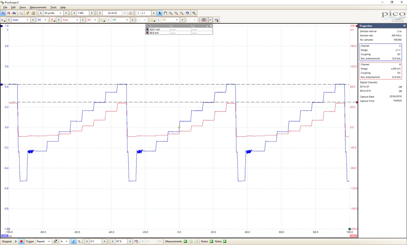
Figure-8: Signal measurement with U1A & U1B disables (Blue is Input & Red is Output)

  • Hi N,

    do all pairs behave this way? Is anything damaged?

    Kai
  • Yes, all pairs behave the same way (I used one pair above to keep the things simple otherwise I have tested all pairs)

    Also, I have used the same opamp for another board which is slightly different configuration (1 input and 2 output opposite to above case) and that board also has same problem.

    There is nothing on board that I could see as physically damaged.

    Kind Regards
    NS

  • Hi N,

    a simulation with TINA-TI shows, that your circuit should work wonderfully...

    Kai
  • Hi Kay

    Thank you very much for your help.

    I am assuming there is No load connected at TINA_TI simulation at the video output!?

    I have not done the simulation but testing the actual hardware.

    The problem I have that with both Amplifiers in each pair Disabled, I am getting considerable Video Signal at the output (with Signal applied to only one input say CH1A (for U1A)), where as if I apply no Signal at one Amplifier say U1B Input and apply Signal at other Amplifier U1A, by enabling U1B I get almost ZERO signal at output which I was expecting I should also get if I DISABLE U1A & U1B (both at same time)

    Is there anything inherently wrong in DISABLE line of this OPAMP?

    Am I interpreting the Disable Isolation Specs correctly?

    Kind Regards
    NS
  • Hi N,

    I have tested with 75R load, 10k load and without load. All simulation were running fine. I have simulated your circuit with connecting the /DIS pin directly to GND and connecting the /DIS pin to GND via resistors. Everything works fine.

    But! If I increase the resistance between /DIS and GND to 1MEG, the output is still disabled, what should not be the case because of the "control pin input bias current" of 2 x 75µA! So, the TINA-TI model seems not to be representative reffering to the /DIS pin and associated internal circuitry!

    Kai
  • Hi Kai

    Thank you very much for your feedback.

    Datasheet says that by leaving /DIS pin floating, amplifier should be enabled. So yes for your simulation case of 1M pull down, amp should have been enabled.

    I was hoping to get some feedback from TI tech support as well on my issue as in the past I have been using FAE support from distributors like Arrow etc which used to be fairly prompt. Unfortunately they are not available anymore and I hope this issue is not going to delay this product too much.

    The fact that problem is persistent across different PCBs makes me think that it has something to do with the actual DISABLE pin control circuitry inside the chip unless I have a bad batch of OPAMPs

    Kind Regards
    NS
  • Hi there

    Anyone who has used this IC and has any feedback on this problem please!?

    As clearly there is contradiction between Simulated results (as kindly done by Kai Klaas69 - above) and the actual hardware!

    Kind Regards
    NS
  • Hi N,

    have you tested the performance with a symmetrical supply, e.g. +/-5V?

    Kai
  • Hi Kai

    No I have not tested it with +/-5V as that would require major design change.

    I thought it should work fine with Single Supply as well!?

    Kind Regards
    NS
  • Hi NS,

    I am taking a look at your issue on the bench, and see whether I can replicate the problem you are seeing. I will post my results sometime later this week as I still need to receive the OPA3692 ICs, which usually takes about a couple of days from ti-store before I can begin my test.

    In the meanwhile, is it possible for you to record supply current of both U1A and U1B when both the amplifiers are disabled? Also in Figure 4 waveform image that you posted, the output you are recording is ~500mV and not 49.9mV correct?

    Is it also possible for you to look at U1A and U1B outputs individually by disabling one amplifier at a time? An experiment to try would be to remove R15 first, disable U1A and see if there is any waveform at the U1A output. Similarly, remove R14 next, disable U1B and see if there is any waveform at the U1B output. I think this would give a clue as to whether the individual amplifiers U1A and U1B are actually being disabled.

    Best Regards,
    Rohit
  • Hi Rohit

    Thanks for the feedback.

    OK I will do the tests as you suggested and post my results.

    Regarding Figure-4 measurement. There are two traces Blue & RED. The Blue trace (Input) has vertical scale shown on the left of the picture which is in Volts. The RED scale has vertical scale shown on Right of the picture which is in mV. So, the output on Red scale is apprx 49ishmV. Whereas Input is Blue scale of apprx 0.42ish Volts

    Kind Regards

    NS

  • Rohit

    As you are planning to test the circuit on bench, here is my full circuit (OPAMPs only) for this boards. Three opamps on left belong to one IC U1 OPA3692, three opamps on right belong to 2nd IC U2 OPA3692

  • Hi Rohit / Kai

    I carried out some more tests by isolating opamps in each pair as suggested by Rohit.

    Some interesting results:

    All the opamps that have a pull-down 10K at the output pin (e.g., R12 on U1A in Figure-1) showed the problem with small signal at output when they were DISABLED. All other opamps (with No pull down 10K on them at the output) showed no signal at the output when they were disabled.

    I added these 10K as an additional safety to discharge output Cap (220uF) e.g., C15 in Figure1 in case there is some charge left across it on the node towards opamp side when the OPAMP is disabled. I thought that this is quite high resistance compared to the load of 150R that opamp would be driving in normal operation (75R + 75R). Having said that all of this is true when OPAMP would be ENABLED. And if this Pull down resistor had any significant impact on the quality of signal, I would have observed it when OPAMP is enabled. I have no such issues (at least for this application) regarding the video quality when OPAMP is ENABLED. But the problem here is that I am seeing a signal at OPAMP output when it is DISABLED. 

    If I remove these pull down resistors from the board, then signal drops down to almost ZERO when the OPAMPs are disabled. (with & without two outputs joined together as in original circuit)

    Another thing I  noticed is that having this 10K pull down at opamp output reduces the DC Voltage level (as measured by DVM) at OPAMP output to apprx 1.38V as compared to apprx 2.47V (for opamps who have no pull down of 10K at the output)

    So, could you please help me in understanding the effect of having this pull down at OPAMP's output when it is DISABLED. (It is R12 in Figure-1 ----- Not the R17)

    Last point (not critical but it would be good to have some explanation to it), at power up when all opamps are disabled, the output after the output CAP (e.g., node CH1 in Figure-1) first goes high momentarily to some voltage and then slowly drops to near Zero. However, if OPAMP is ENABLED and then DISABLED, the output drops to ZERO very quickly as compared to when it slowly drops to ZERO at the Power up with both OPAMPS Disabled. Any idea why it would behave like this (the rate of drop is very slow if opamps stay disabled BUT it increases significantly if they are first Enabled and then disabled)?

    Kind Regards

    NS

  • Hi NS,

    It is good to know that removing the 10k resistor directly connected to the OPA3692 output resolves the disable issue.

    I think it is possible that having the pull-down at op-amp's output when disabled is weakly biasing the device output ON resulting in some leakage from the input to the output. So, you might be seeing the residual voltage due to the op-amps output being weakly turned ON. I would certainly not recommend to use the 10k resistor, as it is not required for video application.

    For the case where the output cap first goes high momentarily to some voltage and then slowly drops to near zero during power up, you are simply seeing impulse response of the output cap. When the device is powered up on single supply, the device output is ramped up to 2.5V which essentially charges up the output cap towards the device side and is subsequently tracked by the output of the output cap. However, once the device output is stable at 2.5V DC, the capacitor is no longer being charged which results in the output of the output cap to decay with time constant = 1/(2*pi*10k*220uF) which is significantly long.

    Similarly, when the device is powered-on and then disabled, the output cap voltage will go to 0V very quickly because the device output is ramping down to 0V within 1us (see page 8 Large signal enable/disable waveform in the datasheet). The fast ramping down of the device output to 0V discharges the output cap resulting in fast ramp of output of the output cap.

    Best Regards,
    Rohit