This thread has been locked.

If you have a related question, please click the "Ask a related question" button in the top right corner. The newly created question will be automatically linked to this question.

TIPD102: The 2nd stage is not functioning as specified when practically tested in lab

Part Number: TIPD102
Other Parts Discussed in Thread: TINA-TI

Hi,

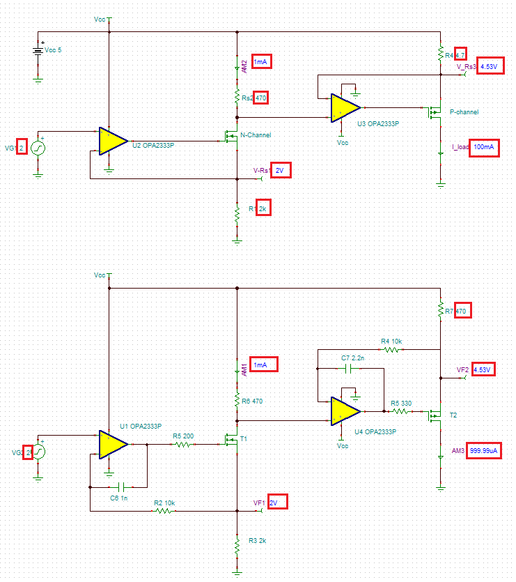
I wanted to use this circuit for my application where I wanted 0 to 1024uA (or 0 to 1mA) current.

I downloaded the gerber files and got it fabricated, and assembled with same components and accuracy as specified in the BOM

Practically, in the first stage I get current output only after 0.3V input, and i.e. 150uA output and from then on it is linear with every step of 2mV increase I get 1uA output step upto 1000uA

Also the second stage does not give me any output. There is no 0 to 100mA output. I have attached the test results for your reference.

After that, since my requirement is 1mA and not 100mA, I have changed the resistor in 2nd stage from 4.7R to 470R, and again  there is no proper response in the 2nd stage of the circuit.

Please let me know solution for the above problems.

Thanks & regards

Krishna kumar C.Fab_Board_testing_Results.xlsx

  • Is anyone out there? I have not received any response for this question? I kindly request the support team to help me at the earliest.

  • Krishna,

    The circuit shown in TIPD102 works properly - see below.

    However, since for the circuit to operate correctly, there is some minimum current required, AM2, to bias N_channel transistor (see N_channel transistor datasheet), you may not apply VG1=0 because under such condition AM2 bias current would be zero (VG1/2k) - see below.

    The second stage does not give you correct output most likely because you either use N-channel transistor instead of P-channel or have not connected P-Channel transistor correctly (source must be at the top).  I have attached here Tina-TI schematic for your convenience.

    Krishna.TSC

  • Dear Marek,

    Thank you very much for the prompt response. Thank you for simulating the circuit and attaching the results. 

    There are two issues in the circuit

    1. Stage 1 issue:

    The circuit, Its all good in simulation, but practically T1 is getting activated only when VG1 or VG2 is around 0.3V, and I am getting a current output of 150uA corresponding to 0.3V, which is linear from 0.3V Input. I am not able to bring down the activation point of T1 to a voltage less than 0.3V, I am stating this after around 2 to 3 weeks of different practical experiments and trials.

    The test results were attached with the previous post, as you had observed.

    2. Stage 2 issue

    Your speculation of connecting the P channel FET incorrectly cannot be true because I have the board fabricated from the gerbers available in TI website and it is correctly matching the footprint and I have practically verified the connections after fabrication, before and after assembly.

    Thanks & Regards

    Krishna