This thread has been locked.

If you have a related question, please click the "Ask a related question" button in the top right corner. The newly created question will be automatically linked to this question.

PGA205: PGA205 circuit issue

Part Number: PGA205
Other Parts Discussed in Thread: OPA192

Hello,

We are trying to integrate the PGA205 IC in an amplifying circuit - the scheme is attached below.

We encounter issues from an unknown source, any help will be appreciated.

The circuit includes two parts of amplifying - first part is an op-amp switching sensor's current to voltage,

which output in scheme can be seen as "TP2". This part includes analog switches for changing the gain rate.

The output of the first part is driven to the PGA205, which outputs can be seen at scheme at "TP1".

The problem is that when switching PGA205 (by A0 and A1) it influences the first part of amplifying,

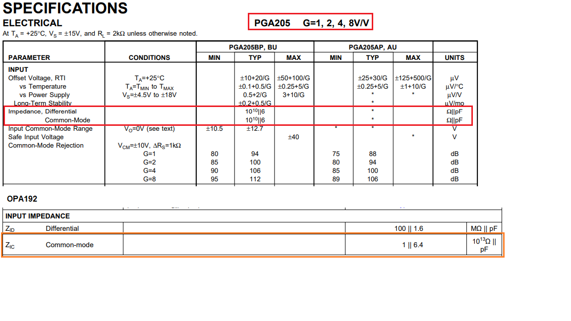
which seem to be due to some undesired capacitance.

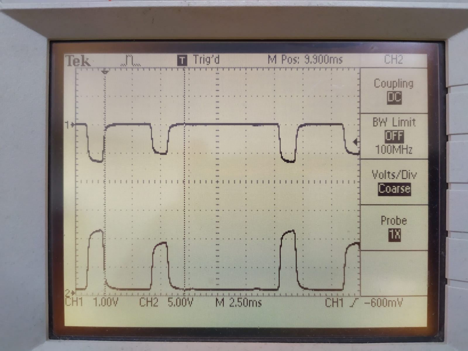
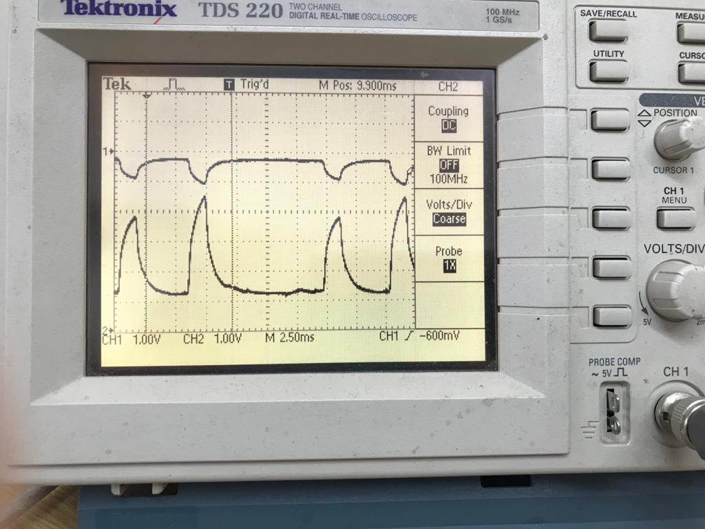
Attached below are oscilloscope views at TP1 and TP2 points, where the top is TP2 (first part of amplifier, I to V), and the

bottom is TP1 (output of PGA205). As can be seen, when changing switch state at PGA205 also TP1 as well as TP2 change rate,

and the signal which should be a trapeze is distorted.

2161.1.pdf

  • Add to Phrasebook
    • No word lists for English -> Hebrew...
    • Create a new word list...
  • Copy
  • Add to Phrasebook
    • No word lists for English -> Hebrew...
    • Create a new word list...
  • Copy
  • Hi Amitai,

    I do not see any outstanding issues with your schematic design from the transimpedance amplifier in OPA192 to analog switch to PGA205. Please make some additional measurement, and let us know the test result. Here is what I am interested. 

    1. TP2 test point is a very high impedance point. Please repeat the same measurement with a low capacitance scope probe. I am wondering if the measurement is artificial due to probe capacitance. 

    2. U4A and UA4B are used to switch gains for PGA205. If the capacitance of mosfets are high, the RC time constant may be significant. But I doubt that this is the issue, since time constant of input signal is around 1.25 msec. 

    3. Please verify that the switch position in DG1413EQ is implemented correctly. There are no cross talk/path among the top and bottom analog switches. 

    4. Please inject a known input current level in square wave at input of J1 connector and see how the rest of circuits are performing. 

    I ruled out PGA205's possible BW issues. At G=2, the BW of the op amp is specified at 400kHz. 

    Please remeasure the signal responses and let us know.

    Best,

    Raymond

  • Hi Amitai,

    Please let me know what is your findings. If the issue is resolved, please let us know as well. 

    thanks,

    Raymond

  • Thanks Raymond for your suggestions,

    Our original circuit, where instead of the PGA205 there is a opamp with switching works proplery,

    so I don't think it because of the prob location etc.

    Attached is the circuit original circuit scheme, may be it can help by comparing between the two.

    Amitai

    15.pdf

  • Hi Amitai,

    This is a difficult problem to diagnose the issues without actual testing results  

    Previously, I requested to inject a known input square wave current signals at input of J1 connector. What were the captured signals at TP2 and TP1. Can you send me captured screen shots?

    My speculation is that it the issues are not likely caused by PGA205. The input impedance of PGA205 is extremely high and input capacitance is extremely low, see the attached imaged. If the same circuit and layout work for OPA192, it is less likely that PGA205 will create the issue. Your signal's RC time constant is approx. in an order of 0.2 msec. 

    I have follow up questions. Please send me the scope screen shots, otherwise  I am unable to assist you. If you have privacy concerns, please send me a private message via E2E forum. 

    1. Do the PCBs in AST-A5-AMP-1001.5 and AST-A5-AMP-1001.6 have the identical layout? What are the PCB layout differences?

    2. In AST-A5-AMP-1001.6 PCB, please remove PGA205 part, inject a known current reference signal in square wave, what do you see at TP2 point? It should follow the input reference signal's shape + gains. Please send me these screen shots. 

    3. How many PCB boards do you observed with the same issues?

    4. From the signal pattern at TP2 at the first stage of I2V, I can see the output of transimpedance signal is already having distortion issues. The amplification of TP2 made worst at TP1 test point after PGA205. My speculation is that your unwanted distortion is somewhere in the first I2V stage, not resulted from the PGA205 gain stage. Please send me the captured screen shots. 

    This is what I am able to suggest without seeing the actual test evidences. 

    Best,

    Raymond

  • Hi Amitai,

    Please let me know the additional findings in your issues. 

    Best,

    Raymond