This thread has been locked.

If you have a related question, please click the "Ask a related question" button in the top right corner. The newly created question will be automatically linked to this question.

LMH6702QML-SP: Optimizing CMRR

Part Number: LMH6702QML-SP
Other Parts Discussed in Thread: LMH6702, THS3217, THS3215, VCA820, OPA695, THS3491, OPA683, OPA684

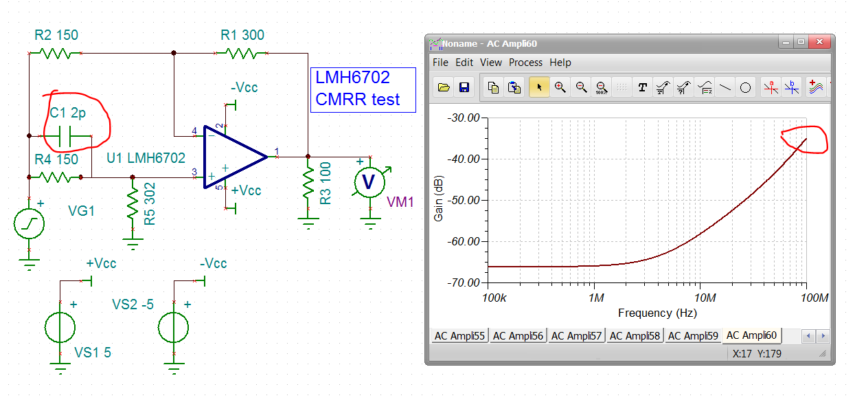
We are using the LMH6702 for an aerospace application and would like to achieve the best CMRR available. I understand one of the demerits of CFAs is poor CMRR compared to VFAs but the typical performance curves on the datasheet indicate 20dB at 100MHz and over 40dB at 10MHz. While these may not seem it would be beneficial to our design if they could be achieved.

I have two questions:

1) can you provide the test circuit used to perform the CMRR measurement for this part?

2) Can you recommend design strategies or methods to optimize the available CMRR? 

Thanks in advance for any guidance you can provide.

Best regards,

Chris Belting

  • So Chris, 

    Your intended circuit would help - but assuming you are doing the typical single op amp diff to single with resistors you can tune the nominal CMRR up by adjusting for the V+ to V- buffer gain loss (which is where CMRR comes from in CFA parts). I think I put that into one of the CFA datasheets I wrote, will look a little tomorrow. 

    In the meantime, we tried pretty hard to get a good CMRR in the input stage for the recent THS3217. You could consider that solution with the 2nd stage disabled to save power. One app I had in mind defining that device (and the lower power THS3215).

  • Yea, here is that D2S CMRR plot for the THS3217, not as good as I remembered but it is actually pretty hard to get good high F CMRR, 

    The other place I worked on this problem was tuning the input CMRR for the wideband VCA820 or 821 VGA's - that gave really good results - will see if I can find that CLC520 base app note tomorrow as well, 

  • Hi Michael,

    Thanks for the prompt response. Unfortunately since we're working in aerospace the parts we can use are limited, and even more so for this project.

    I appreciate you digging up the information you've written as that may be helpful to understanding the issues involved.

    Still, if I could see the test circuit it may be quite informative.

    Our design tries to create a differential amplifier but simulations may suggest not even 20dB rejection around 40MHz. At issue is a sensor contained within a chassis and a remote power supply referenced to secondary ground. Chassis, ground, reference ... I know, I'm just using these names to describe multiple ground domains. Suffice to say our sensor is wrapped in one domain and the amplifier is powered by a different domain. Back at the electronics they're the same but make the connection has multiple cables (power, analog signals, and shields, to and from multiple circuits) and we're left with the sensor amplifying the local difference between ground domains with the same gain as the signal we're trying to measure.

    Hence we would like to intelligently use the LMH6702 and achieve the best CMRR we can get. If it were 20dB at 100MHz that might be fine.

    All the guidance you provide will be helpful and much appreciqated.

    Thanks again

    Chris

  • Ok Chris here is a starting point

    This appears in a lot of the CFA datasheets I did, this one from the OPA695 page 36. This shows where the CMRR comes from, the buffer gain loss (<1) from V+ to V-

    So, to equalize in the diff amp R configure

    1. Increase the resistor to ground on the V+ input slightly to get DC compensation of that alpha

    2. Add a lead cap across the series R into the V+ input to get AC equalization of the buffer rolloff. 

    This all simulates real well, 

  • Morning, before I head out this AM, here is what I mean (somewhere I have the algebra for this, not looking now)

    The Response mismatch in the non-inverting path has a DC gain loss due the buffer gain <1.0000

    It has a couple of poles not in the inverting path due the input parasitic C and the Buffer rolloff

    THe model often captures this pretty well, 

    Here is the nominal matched R (gain of 2) CMRR sim showing what you see in the datasheet, 

    Then, tuning the R to ground for DC improved CMRR (does not help AC), 

    Then adding a speed up cap to cancel the pole (about), this looks promising and is actually pretty repeatable part to part, 

  • This looks very helpful Michael, thanks.

    It's difficult to say how much flexibility we will have to make fine adjustments but knowing what is required definitely helps understanding the issue.

    I'm a little surprised it's not discussed much in literature - I guess I should have been reading other CFA datasheets. 

    If you do find the math, when you get a chance, it should help to wrap up this question.

    Any good literature (references) you could recommend would also be welcome.

    I'm thoroughly impressed by your understanding of the problem and responses. 

    Best regards,

    Chris

  • Thanks Chris, back now, did a little 4 wheeling this AM to pass the time in a safely social distancing fashion. 

    well, as the IC designer on one of the 1st CFA (CLC400) I felt like I needed (at that time, to get a little street cred with all the HP instrument designers around me at Comlinear) to work out the transistor level equations (hybrid pi model) for all these kind of VFA specs applied to CFA - as it turns out, that exercise is useful in defining new parts - 

    Hence, when it came time to define the THS3491, never going to be used at gain of 1 (or shouldn't anyway, always exceptions), so we can burn some headroom on the V+ input stage, appyling a cascoded current source to increase its output impedance biasing those input Q  - one way to incrementally move the buffer gain closer to 1.000. 

    The other way we did some years back was to do a closed loop input buffer (I am part of the patent on that one), the OPA684, OPA683 family. 

    These both have about the highest CMRR for a CFA due to buffer gain getting closer to 1.000

    But really CMRR does not come up that much on CFA apps. 

    And again, if you get into your circuit and layout and impirically find those R and feedforward C values, they likely will be pretty repeatable as the buffer response and input C are pretty repeatable. 

  • Some product history, 

    The LMH6702 is the VIP10 migration of CBICV2 CLC449 - except for ADI, most of us did not have fabs and used Lucent Reading. They started to shut down (due to egregious mismanagment) in the 2000 timeframe where most everyone saw that coming and developed their own internal 12V 10G complementary processes to migrate to - I managed the migration of the BurrBrown OPA product line to CBC10 while what was left of the Comlinear team in Ft. Collins moved everything onto VIP10 in Arlington, TX for National. 

  • Hi Chris,

    if I understood you correctly, you want to route the sensor output to the one input of differential amplifier and the remote signal ground (sensor ground) to the other input of differential amplifier? In this case source impedance matching might be useful. Do you know the source impedance of sensor versus frequency?

    Kai

  • Hi Kai,

    (My first response has disappeared in the ether … too many thumbs perhaps.)

    Your understanding is correct. The sensor is an electron multiplier and the output is ideally a current source terminated with a 50-ohm load resistor to convert the signal to a voltage pulse. I understand your question and have previously seen where including the source resistance in the balanced resistance at the input of a differential amplifier is necessary to achieve the best CMRR. I'm less certain whether this remains true for the CFA since there is a significant difference between the input impedance of the inverting and non-inverting inputs. I would be interested in hearing your thoughts.

    Regarding the impedance vs. frequency, we've made no effort to verify the load resistor's impedance over frequency. The signal gain is intended to be -2 so the sensor load resistance is significant with respect to the values of the gain resistors. If you have additional guidance I would love to hear it.

    Thanks for asking.

    Chris

  • Hi Chris,

    I think Michael can much better explain how to find the proper passive components when designing a differential amplifier with the LMH6702.

    My general tip is: I would do most of the signal processing close to the sensor itself. The higher you can amplify the sensor signal and the narrower you can limit the bandwidth, close at the sensor, the better the overall CMRR.

    Kai

  • Perhaps Kai, 

    The PMT 50ohm impedance is floating out there - I visited Hammamatsu once (out in the middle of rice fields, very picturesque) and tried to extract what that meant? Don't recall succeeding. In any case, if there is an actual source impedance of 50ohms that becomes part of your source impedance into the V+ input. If you think about holding >50dB CMRR, you are headed towards 0.1% R's and that source R is part of that.