This thread has been locked.

If you have a related question, please click the "Ask a related question" button in the top right corner. The newly created question will be automatically linked to this question.

OPA857EVM-978: Test Mode OUT & OUTN Voltages Doesn't Change with DC Bias

Part Number: OPA857EVM-978
Other Parts Discussed in Thread: OPA857

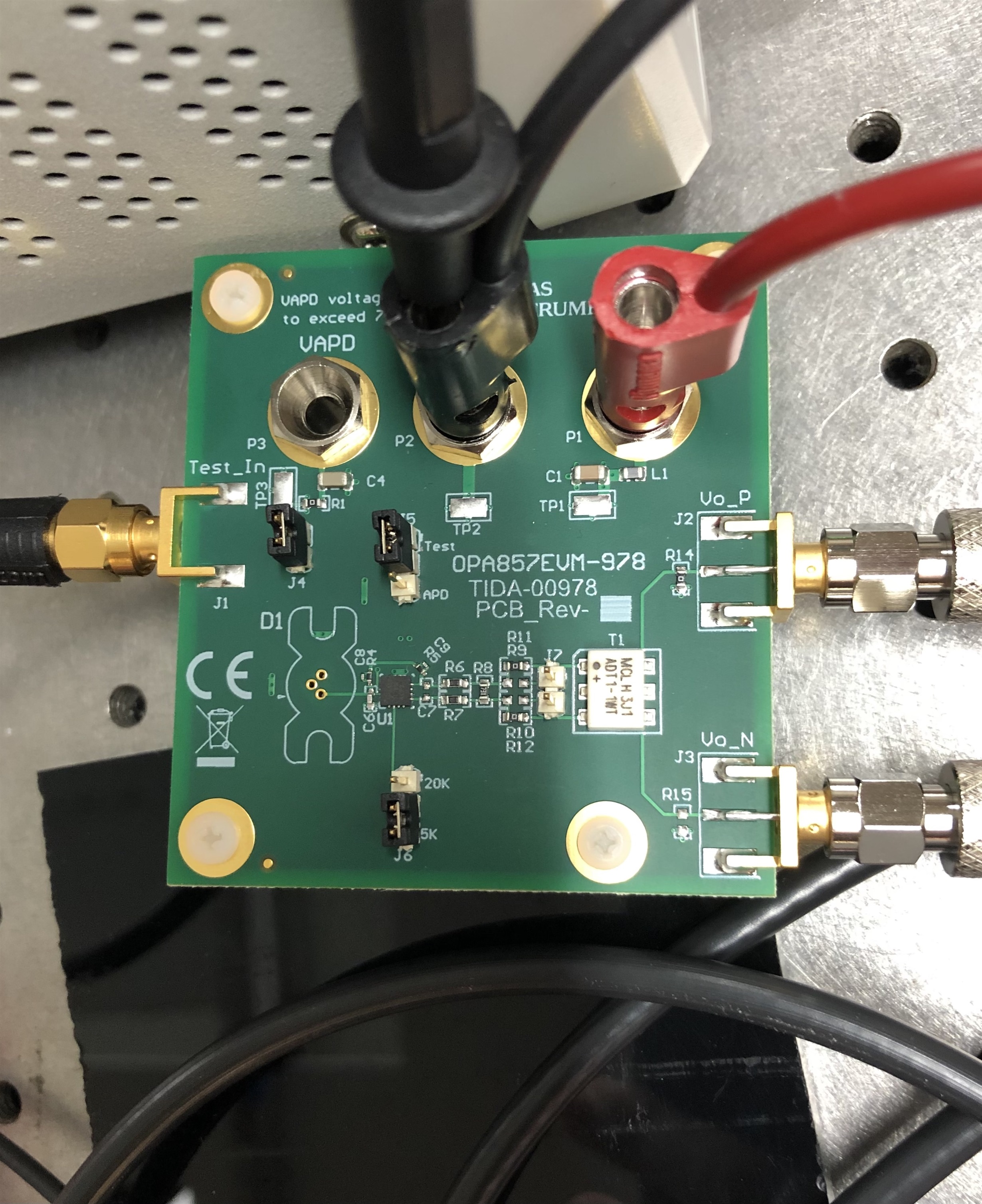
I'm trying to figure out the test mode right now, and the connection is as follows and I've attached a pic for the board:

  • I've connected the TEST_SD pin to Vs to configure in test mode
  • I have 3.3V connected to Vcc from a DC power supply
  • Ground connected to the power supply ground
  • I have the signal generator connected to the Test_in SMA connector
    • 0.5Vpp for the amplitude and I vary the DC bias voltage
  • Vo_P connected to the oscilloscope to observe the output

My question is that the voltage I measured on OUT & OUTN (from the positive side of R6 & R7) are 3.03V & 1.84V. However, while I change the DC bias voltage (keeping the 0.5Vpp amplitude), the voltages of these two nodes don't change at all, and the OUT voltage seems way too high comparing to the approximately 1.33V from the spec sheet. So I'm wondering what have I done wrong or the board is defective?

Thanks,

Xiechen

  • Hello Xiechen,

    The issue is likely due to J4. You need to remove this jumper which ties the test input to VCC.

    Best,

    Hasan Babiker

  • Hi Hasan,

    Thanks for pointing this out and now I've obtained different voltage readings on OUT while adjusting the bias voltage.

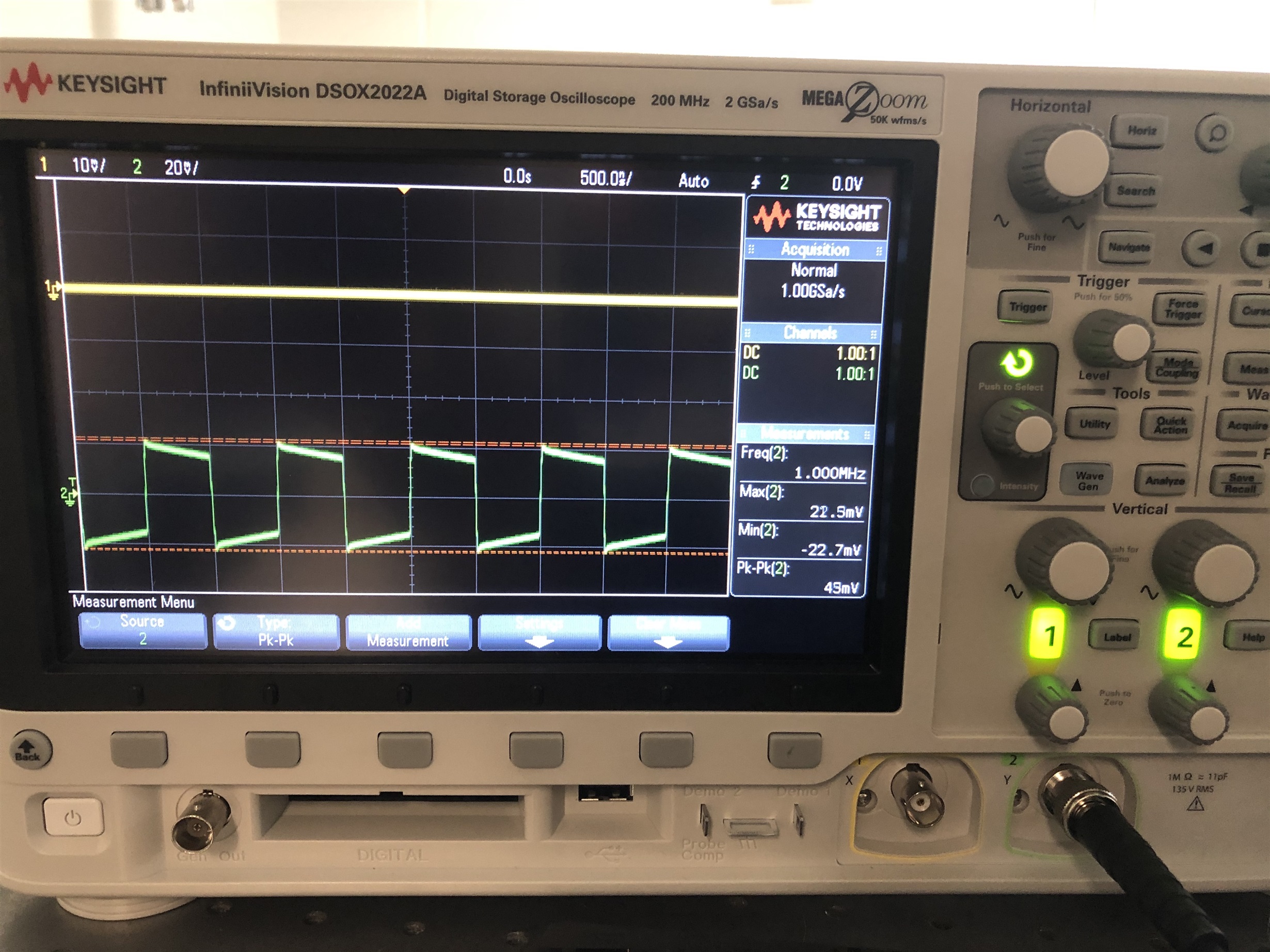
    Now I've identified VIN1 = 2.18V and VIN2 = 1.77V, so I've set the Test_in to be a square wave with 1 MHz, bias voltage to (2.18 + 1.77) / 2 = 1.98V with 0.5Vpp amplitude, but for the output I observed no signal on Vo_P, square wave signal on Vo_N but with low amplitude, shown in the picture below. 

    So I'm wondering what's the issue with no signal from Vo_P, or what should I expect to see there, and why the amplitude from Vo_N is low (I thought the amplitude would be amplified to some extend). Shorting the jumper J7 doesn't seem to change anything, but changing the jumper J6 to 20K increases the peak-to-peak voltage of Vo_N to 76mV (still low).

    Thank you.

  • Hello Xiechen,

    Note Vo_P is currently grounded, it is not meant to produce an output (so you can get single-ended output from transformer). Note that because of the transformer you will need to measure at R11 to find Vin1 & Vin2.

    Best,

    Hasan Babiker

  • Hi Hasan,

    There are couple of terms that I'm not too sure that I understand properly.

    1. What is the common-mode output from the REF block = 1.83V referring to exactly? Does this mean that the voltage I measure for R7 in respect of Ground is 1.83V (I measured this same value on the board consistently)?
    2. When you say adjust the DC bias, should I set the VIN as DC voltage only, or I should make it AC with 500 mVpp. These two situations have different voltages when I measure OUT.
    3. In order to measure the voltage for Vo_N as DC voltage, which node should I measure? The datasheet links the node to R14, but on my board it's connected to R15 (shown in the pic in the original post). Although even I change the DC bias voltage, I cannot obtain a reading from R15 resistor in respect of ground, and I can still observe the square wave output as shown from the previous reply.

    Thanks. 

  • Hello,

    1. This is referring to the reference block within the OPA857. Yes you can measure this at R7 (OUTN of OPA857).

    2. Referring to DC voltage only here. Once you know Vin1 & Vin2, your AC signal should have an amplitude of Vin1 & Vin2 once these are found.

    3. Sorry about the confusion, please use initial instructions on the user's guide rather than my previous response... will edit previous response to reflect this. You will want to measure at R11. 

    Best,

    Hasan Babiker

  • So back to my earlier reply.  I found VIN1 = 2.18V and VIN2 = 1.77V, but their difference is only 0.41V. So for the AC signal, should I use 410 mVpp instead of 500 mVpp for the amplitude?

    Also my main question regarding on the test mode is that what output should I be expecting? I'm observing 70 mV of peak-to-peak voltage from the Vo_N output, which is quite smaller than the Test_in voltage. Is it normal or I should expect something else?

    Thanks.

  • Hello,

    Yes that is correct you should use 410mVpp at the input if these were the correctly measured Vin inputs to achieve a 500mVpp at DC. Can you measure the output at R11 with the 1MHz signal? Does your amplitude increase at Vo_N if frequency is increased?

    Best,

    Hasan Babiker

  • What do you mean by "measured Vin inputs to achieve a 500mVpp at DC"? I obtained the Vin1 & Vin2 values when OUT voltages are 1.33V & 1.83V. 

    I connected Vo_N to the oscilloscope directly and the amplitude doesn't change with the change of input frequency. 

    I'm out of the lab right now so I can't measure the output at R11, but should I be using a multimeter to do the measurement or I should probe it to the oscilloscope?

  • Hello,

    If you are measuring at OUT(pin 8 of OPA857) of the amplifier then the signal should be attenuated. See below:

    Note the attenuation that occurs as a result of R6/7 & R8.

    Best,

    Hasan Babiker

  • In the user guide it says "Adjust the DC bias of VIN2 until OUT = 1.83 V - 0.5 V = 1.33 V for a 500-mVPP output swing. OUTN remains constant at 1.83 V." This is what I did as I applied VIN2 = 1.77V to get the DC voltage at OUT to be 1.33V.

    The output signal is connected from Vo_N to the oscilloscope directly using SMA to BNC connector.

  • Hello,

    The 500-mVPP referred to here is at the output of the OPA857. You will either need to increase your input or remove attenuation following the OPA857 to achieve this at Vo_N.

    Best,

    Hasan Babiker

  • Hi Hasan, Thanks for your time.

    • How can I increase the input if Vin1 & Vin2 are fixed after following the steps to have OUT = 1.33V, and therefore the amplitude would also be fixed?
    • Remove attenuation as removing the resistors R6/7, R8, or through other means?
  • Hello Xiechen,

    • You will have to adjust Vin1 & Vin2 to satisfy your output requirements. Note that the lowest the OUT pin will go is at around 0.6V.
    • That is correct, removing resistor R8. Or replacing these resistors to meet your attenuation requirements.

    Best,

    Hasan Babiker

  • Hi Hasan,

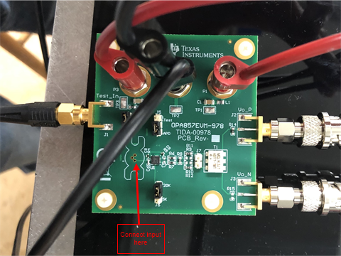
    Thank you for the response. Now I'm trying to connect the photodiode and try to observe the outputs in photodiode mode. I've attached the board connection here.

    • Photodiode is battery powered, without built-in amplifier (ThorLabs DET210). I used 532nm green light for the photodiode and there's 12V, 0.1mA from the photodiode output, connected to the VAPD port.
    • Test_in is connected directly from DC supply (3.3V), and J4 jumper is shorted. J5 jumper shorted with APD.
    • The gain is switched to 20k

    However I observed no signals from either of the outputs (Vo_P & Vo_N). Do you know what's going on here? I think there's enough current generated from the photodiode. Thank you.

  • Hello Xiechen,

    VAPD is supposed to be used to bias your photodiode, and isn't that photodiode input itself. 

    This EVM is designed for a TO-CAN photodiode.. you will need to connect your input signal to the highlighted pin.

    Best,

    Hasan Babiker

  • Hi Hasan,

    Thank you for your reply and I will need to place an order for this type of photodiode. I will mark this post as resolved and if I run into other issues after plugging in the TO-CAN photodiode I will create another thread.

    Xiechen