This thread has been locked.

If you have a related question, please click the "Ask a related question" button in the top right corner. The newly created question will be automatically linked to this question.

TLV2460: Driving capacitive load directly (no AC component to the signal)

Part Number: TLV2460
Other Parts Discussed in Thread: TINA-TI, TLV2464, AMC1200, TL431

Hello everyone,

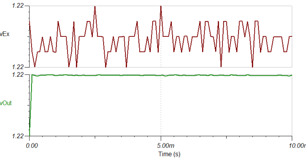
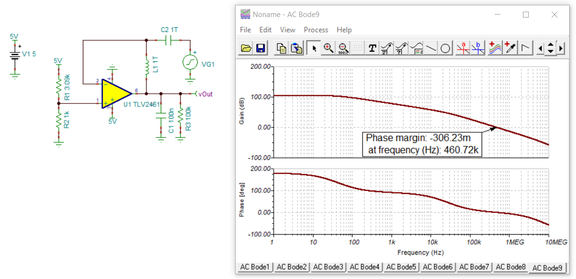
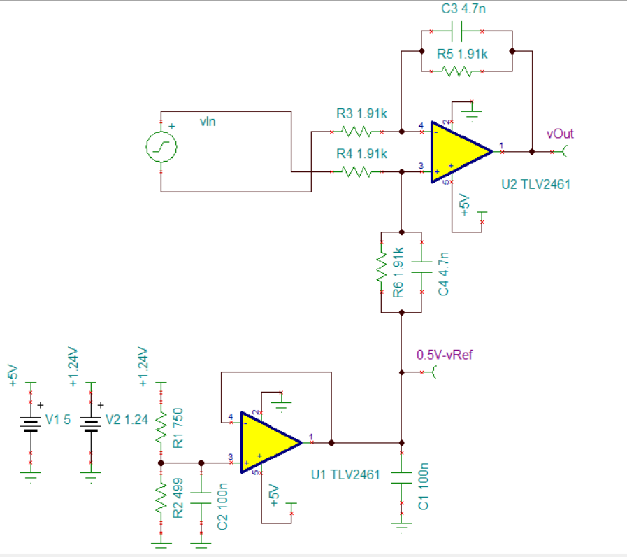
I have inherited a circuit in which multiple reference voltages are derived from a single reference voltage: resistance divider outputs are buffered with TLV246x opamps. 0.1u bypass capacitors are placed at the opamp outputs.

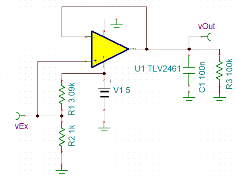
Normally, one wouldn't place a capacitor directly at the opamp's output. However, circuits such as above seem to work fine. There is no AC component to the output voltage, but I am not sure if the current out of the opamp is purely DC (I have put a 100k in the simulation above just to have some load).

Is this method fundamentally unstable? Should there be a resistor, let's say 10-100 Ohms, between the opamp and the capacitor even if it drops a few mV?

Thank you.

-ST

  • In case it is helpful to see the simulation result (I chose Transient > Calculate OP):

  • Former Member
    0 Former Member in reply to Saurabh Tewari

    Hello Saurabh,

    It is true that it is not a good idea to hang larger capacitive loads (probably greater than 1nF) without some type of stability compensation.  With the higher capacitive loads, the interaction of the capacitor with the output impedance of the amplifier can create a low frequency pole which can creep into the bandwidth of the amplifier, reduce the phase gain, and lead to an unstable circuit.  It seems like you are aware of this.

    The question, and it is a good one, is whether this can be a problem when the circuit is just acting as a voltage reference.  We recommend ensuring your voltage references are also stable because if there is a small, temporary change in the voltage levels it can create an unwanted oscillation in the output.  If your system is really unstable, the output may oscillate uncontrollably.  Small changes may happen due to noise, current surges, rapid supply drops, etc.

    I went ahead and ran a stability simulation on your circuit.  As expected, the phase margin is non-existent.  I'd recommend considering some compensation.  There are other ways of doing this if adding an isolation resistor leads to an unacceptable voltage drop.

    Let me know if you'd like me to point you to some more resources on compensation techniques for unstable op amp circuits.

    Regards,
    Daniel

  • Former Member
    0 Former Member in reply to Former Member

    Hello Saurabh,

    My first attempt to upload the image did not work.  Here it is again.  I have also included the TINA-TI version of the simulation I ran.

     TLV2461_stability.TSC

    Regards,
    Daniel

  • Thank you Daniel for the thorough explanation. Yes, it would be great if you could point me to the possible compensation circuit(s).

    Regards,

    Saurabh

  • Former Member
    0 Former Member in reply to Saurabh Tewari

    Hello Saurabh,

    Please see this link and scroll down to presentations 10.5 and 10.6.  They are the fifth and sixth presentations in the series on op amp stability and cover the isolation resistor and isolation resistor with dual feedback techniques.  The first is much simpler to design and a bit less prone to errors due to component variation.  However, the dual feedback avoids the problem of a small DC offset across the isolation resistor.

    If you do not have time to watch the videos, the presentations are also available in PDF format with the spoken text and slides shown.

    Let me know if you have any further questions.

    Regards,
    Daniel

  • Thank you Daniel, this is very helpful. Certainly something to keep in mind for the future. I have a more immediate question about this capacitive loading that I could use your advice on. Below is the circuit diagram of the amplifier that uses the generated reference voltage. I have made it as close as possible to the actual circuit that we are using.

    The 1.24V is generated by a TL431. The 0.5V is generated by a resistance divider and then buffered by one of the four opamps of TLV2464. The 0.5V is then used as the offset voltage on a difference amplifier realized by another opamp of the same TLV2464. The inputs to this difference amplifier are coming from an AMC1200 type isolation amplifier.

    In the diagram above, the value of C2 is not important whereas C1 is loading the output of U1 directly. My question is if it is better to just remove C1 from the PWA? I am also including a screenshot of the layout below. As you would see, the 0.5V trace (highlighted) is small and I don't think that having C1 (C106 in the actual board, highlighted below) serves much of a purpose:

    Thank you for your help.

    Regards,

    Saurabh

  • Former Member
    0 Former Member in reply to Saurabh Tewari

    Hi Saurabh,

    I am happy to hear your found the information helpful.  If you just have a discrete capacitor on the output, I don't see an advantage to doing that.  If you want to filter out certain frequencies, the simplest way to do so would be an RC filter at the output, which would involve adding a resistor.  Generally, capacitive loads are not added in with a discrete component but are the result of loading from another component, cable, instrument, sensor, etc.  So, if there is no known purpose for the capacitor, I would remove it.

    C2 is probably ok because of R1, though a simulation can be run just to be sure.  In this case, I would think you'd get some high frequency filtering though I am not sure how necessary it would be.

    Regards,
    Daniel

  • Former Member
    0 Former Member in reply to Saurabh Tewari

    My pleasure Saurabh!  Feel free to post again if you require any further assistance.

    Regards,
    Daniel