This thread has been locked.

If you have a related question, please click the "Ask a related question" button in the top right corner. The newly created question will be automatically linked to this question.

PGA281: Gain Linearity issue

Part Number: PGA281
Other Parts Discussed in Thread: ADS1259,

Hi,

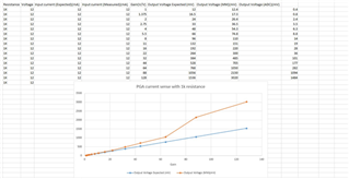
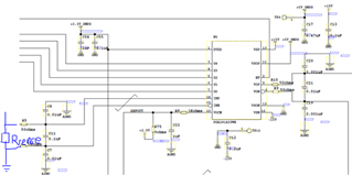
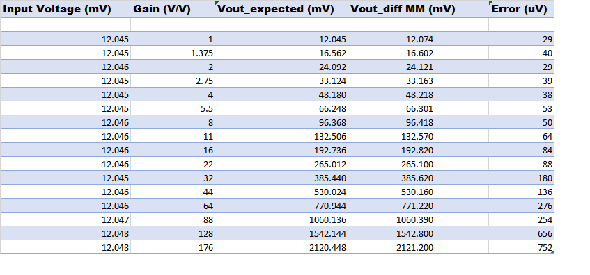
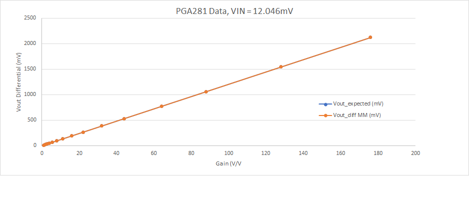
I was hoping you could provide some clarity on the reading I am getting using a PGA281 in a low side current sense configuration. The readings seem to be relatively accurate and linear where the gain settings are set low 1V/V to 64V/V however at around the 88V/V gain setting there seems to be a substantial jump. R-sense for this example is set to 1 Ohm using a relatively accurate . I have looked at the data sheet but cant really make any sense of this (no pun intended). Thanks in advance for any help. 

  • Hi Helder,

    what tells the error flag?

    Kai

  • Hi Helder,

    The table image with the output voltage plot and input voltages is blurry; I can't read it.

    Can you please attach a word file or excel file with the input voltage vs output voltage when the non-linearity occurs with gain of 88V/V?  When you create this table, can you also confirm or include a measurement with the input voltage across the IIN and INP inputs with a high precision external meter when the non-linearity issue occurs?  Is this occurring on a single PCB with one PGA281 device or is this occurring on various PGA281 devices?

    Thank you and Regards,

    Luis

  • Hi Luis,

    I have not measured voltage across the Resistor, but I will do so shortly. In the meantime please see attached. 
    7485.Doc1.docx

  • Hi Helder,

    Thank you for the word document with the data.  The max RTI (referred to input) offset of the PGA281 is ±(20+235/G) µV or 22.67uV at room temp with G= 88V/V.  The temperature drift of the device is quite small, in the sub-microvolts per degree Celsius and the max gain error expected is 0.15%.  The gain non-linearity error is 15ppm maximum.

    If I interpreted the word document plot correctly, the data shows very large errors. 

    For example, an input voltage of 12mV (Rsense=1-ohm*12mA), and PGA Gain = 88V/V should yield a nominal PGA output voltage of 1.056V and the worst accuracy uncalibrated error expected should be roughly ±1.6mV, (1.0544 to 1.0576) after adding the worst-case gain, offset and non-linearity error.   The data appears to show ADC output of 1,094V and additional column shows “output voltage (MM)” of 2,150 mV.

    I don’t see any obvious issue on the partial schematic provided, but I am missing the complete schematic.  

    I have a few questions:

    • On the word document, what does “Output Voltage (MM)” mean? and what is the difference against “Output Voltage ADC”? Are these voltage meter measurements?
    • Can you verify the PGA281 input voltage with an external high precision 6 ½ resolution voltage meter? Please measure the voltage with the meter probes right at the IN-N and IN-P input pins of the device. Please also confirm with an oscilloscope that the voltage input is stable and no oscillations are present.
    • Please verify the PGA281 output voltage with an external high-precision voltage meter. Please measure the voltage right at the VO-P and VO-N output pins of the device. Please also confirm with an oscilloscope that the output voltage is stable and no oscillations are present.
    • What ADC device are you driving with the PGA281? What is the sampling rate, resolution, timing and accuracy on the ADC device?
    • Is the issue occurring on one single PGA281 device or varous PGA281 devices? If only one device has been measured, can you swap the device? 

    If you wish, we would be happy to review the design if you provide a complete schematic and PCB design layout.

    Thank you and Regards,

    Luis

    • DOC1.xlsxOn the word document, what does “Output Voltage (MM)” mean? and what is the difference against “Output Voltage ADC”? Are these voltage meter measurements?
      • MM is output voltage measure by out 6.5 Digit  Multimeter Vs Out put measured by out ADS1259.
    • Can you verify the PGA281 input voltage with an external high precision 6 ½ resolution voltage meter? Please measure the voltage with the meter probes right at the IN-N and IN-P input pins of the device. Please also confirm with an oscilloscope that the voltage input is stable and no oscillations are present.
      • See attached DOC I have performed the measurement right at the input pins.
    • Please verify the PGA281 output voltage with an external high-precision voltage meter. Please measure the voltage right at the VO-P and VO-N output pins of the device. Please also confirm with an oscilloscope that the output voltage is stable and no oscillations are present.
      • Again See Attached DOC
    • What ADC device are you driving with the PGA281? What is the sampling rate, resolution, timing and accuracy on the ADC device?
      • As Mentioned above it is the ADS1259IPW set to the lowest sample rate for highest accuracy. 
    • Is the issue occurring on one single PGA281 device or various PGA281 devices? If only one device has been measured, can you swap the device? 
      • I have only Loaded 1 PCB for now, however I have replaced the PGA281 as I though it may have been faulty, this however did not rectify the problem. 
      • I Would be happy to provide you with the design files if you PM me with your email.
  • Hello Helder,

    I have sent you a friend request so we can share the schematic via private conversation.

    I will get a hold of the PGA281EVM and produce measurements with the G=88V/V.  Please allow a couple of days.

    The partial schematic shows different ground symbols: AGND and GND.   The VSP/VSN supplies and the output stage supplies are referred to "GND". The RSense resistor and filters are referred to the "AGND" symbol. 

    Can you please confirm: is "AGND" and "GND" on the schematic joined or connected together somewhere in the schematic? Are these grounds at the same potential?  If they are not at the same potential or not connected, can you please connect them and let me know if this helps with the issue?

    Thank you and Regards,

    Luis

  • Hello Helder, 

    I went ahead and set up the PGA281EVM on the bench, applying a DC source (B2912 Source/measure unit) and measure the voltage across the inputs and outputs using two 6 ½ digit multimeters and changing the gains.

    IN-N =0V (GND), IN-P = ~12.047mV, VSP/VSN = ±15V, VSOP=+5V, VSON=GND, VOCM=+2.5V.

    Below is the table with measure results, where the absolute error is in the 10's to 100's of microvolts.  This accuracy error is within the offset, gain, common-mode and linearity errors of the device.  No gross large linearity error is seen at the higher gains on the EVM; and the expected output and measured output voltage track closely..

    One possible problem that comes to mind is a grounding issue.  In the schematic, if the supply ‘GND’ and ‘AGND’ in the schematic are not connected together to the same 0-Volt potential, it is possible that the device is outside the input voltage range.  Both IN-P and IN-N inputs of the PGA281 need to remain within the allowed voltage range.  If the Rsense resistor is not grounded to the same potential, it may be possible that the inputs are just at the edge, or outside of the valid input linear range, and a gross linearity issue will manifest as the gain of the instrumentation amplifier is increased:

    (VSN)+2.5V < Input Voltage Range < (VSP)-2.5V

    I have sent you a request for private conversation, in case you would like to share the schematic and PCB layout for review.

    Thank you and Regards,

    Luis