This thread has been locked.

If you have a related question, please click the "Ask a related question" button in the top right corner. The newly created question will be automatically linked to this question.

AMC1100: Analog Signal Conditioning Circuit

Part Number: AMC1100
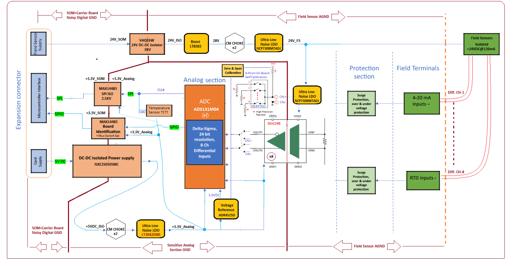
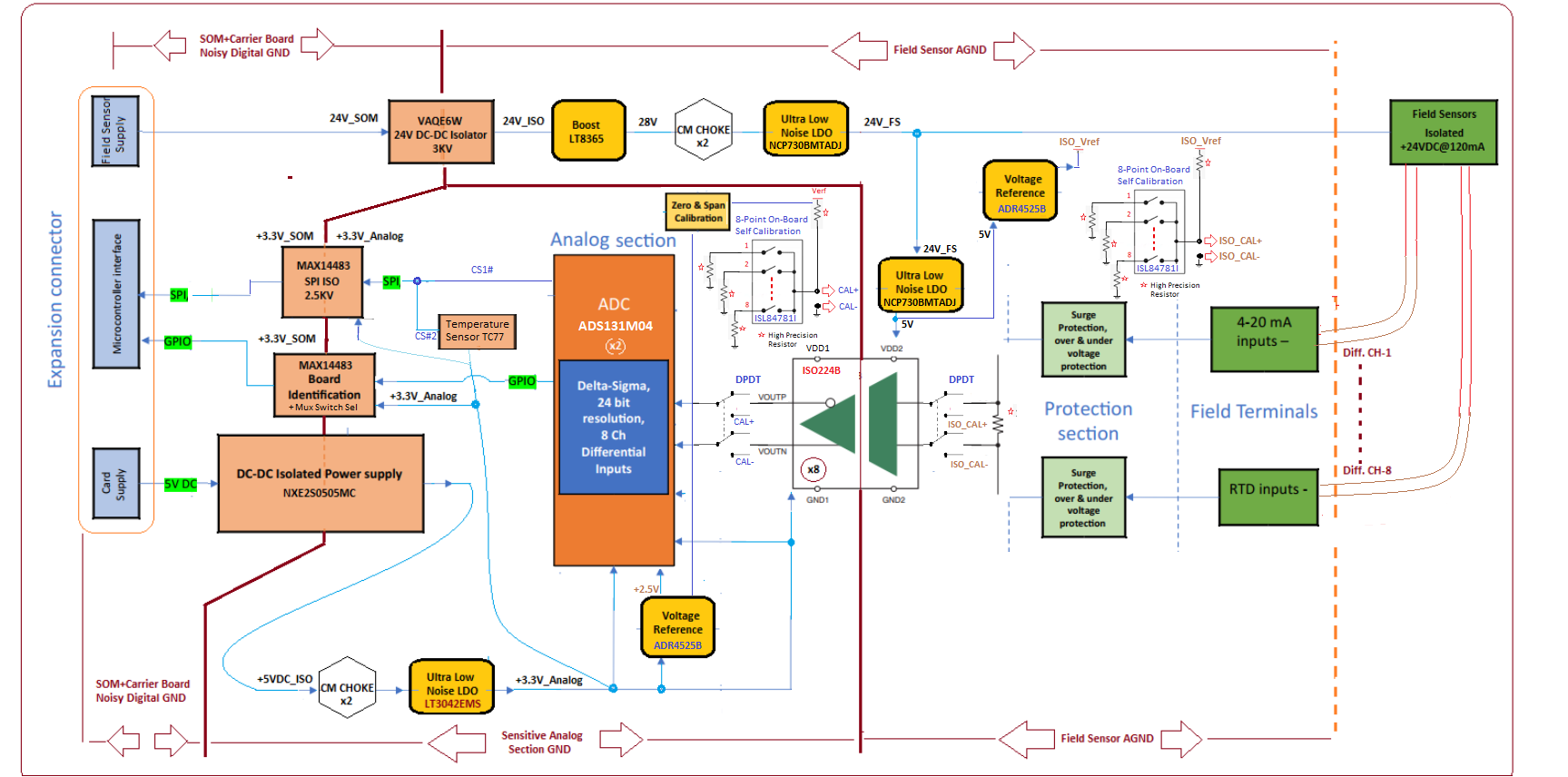
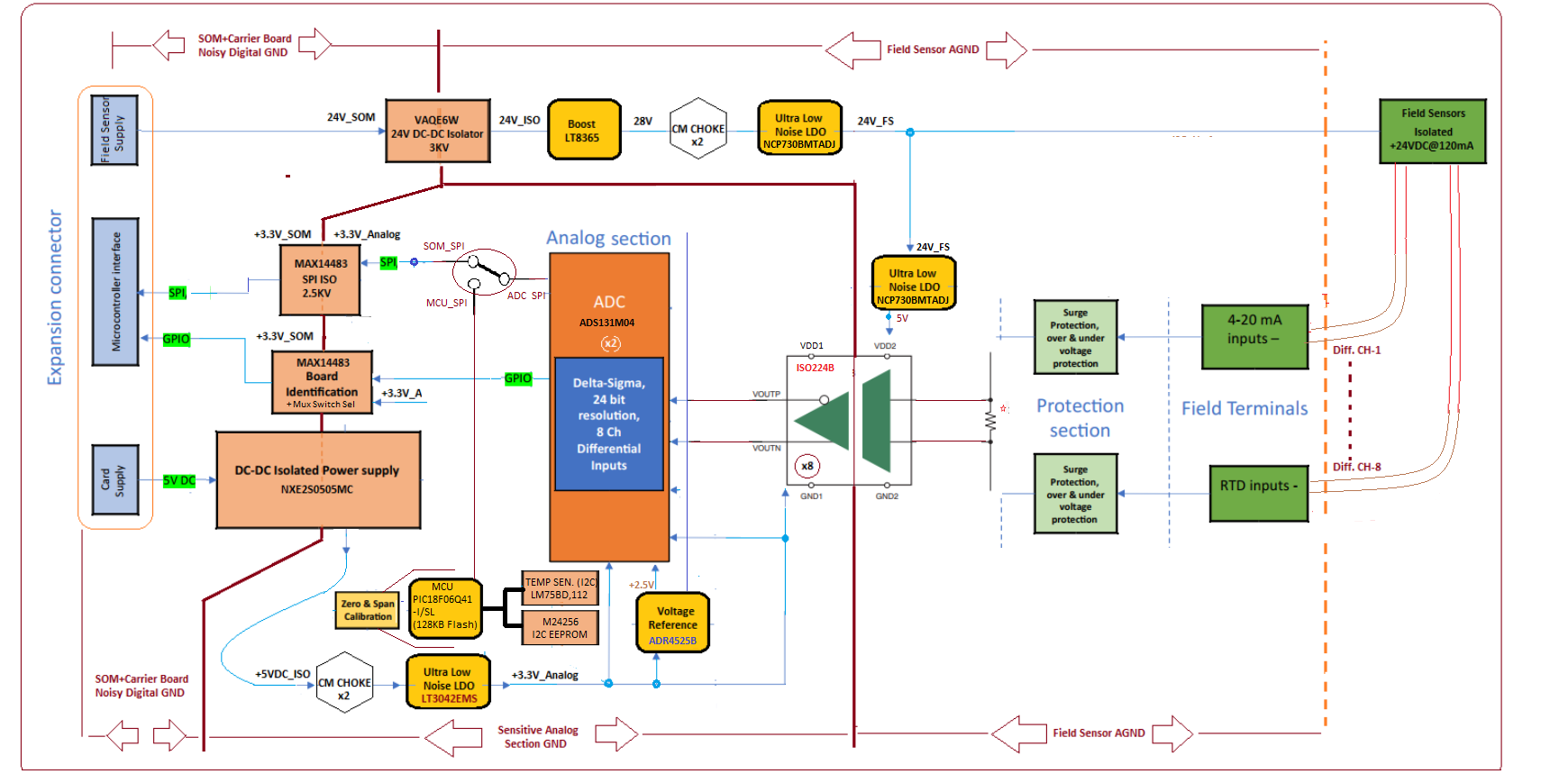
Other Parts Discussed in Thread: ADS1234, XTR105, ISO124, RCV420, , ISO224, AMC1336, ADS131M04, ADS131A04, ADS131E04, REF70, REF7025

Dear Sir/Madam, 

We have below specification from client to sense Analog inputs. We are planning to use TI's ADC : ADS1234 for this project. 

**********************************

• 8-Ch Differential Analog Inputs.
• 4/8 - Ch (Analog inputs: 0-5Vdc, 1-5Vdc, 4-20mAmp, 0-20mAmp). Accuracy <0.008% FS. On board 250 Ohm shunt resistors -selectable for mA type inputs. Input impedance 1MOhm for mV type inputs.


• 4/8 – Ch (RTD input – PT100 type). -140 - +220 deg. C. for 100 ohms input. Resolution 0.01 deg. Celsius. In the same design these
4 Ch can also be selectable as Analog inputs (Analog inputs: 0-5Vdc, 1-5Vdc, 4-20mAmp, 0-20mAmp). having same specification
specified in above point

**********************************

We need best Analog Front End's cost effective solution from isolation and accuracy point of view. From below two options which option we need to select and what are PROS and CONS between two options. We need to submit quotation to client by end of tomorrow. Your earliest response will help us lot. 

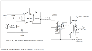
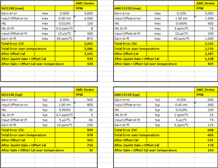
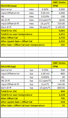
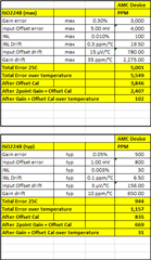
Option : 1 We will go with ISO124+XTR105+RCV420 combination as per shown in attached reference design image.

Option : 2 We will go with AMC1100 Fully-Differential Isolation Amplifier


  • Hi Himanshu,

    I am not familiar with XTR105 or RCV420, I only support the AMC1100 and ISO124 so I can speak to both to these devices. 

    Both the AMC1100 and ISO124 are older devices and we have newer devices available in both of their spaces. 

    The ISO124 is intended for high voltage sensing with a +/-10V input. The ISO224 is the newer version of the ISO124 and has the advantage of not requiring bipolar power supplies and higher accuracy. The AMC1100 is intended for current sensing with a +/-250mV input, low input impedance input. This device can be used for voltage sensing as well, but the small input range is not suitable for high voltage measurements where system noise may greatly impact the measurement and does not meet your 1Mohm criteria. 

    I recommend that you take a look at the AMC1211. This device is intended for unipolar measurements and has high input impedance. 

    What is the desired level of isolation performance? Basic or reinforced? 

    Accuracy <0.008% FS is a very accurate specification, requiring 14 noise and error free bits. What kind of calibration are you planning on performing for the system? 

    You may need to consider upgrading to an isolated ADC such as AMC1336 for higher performance, or consider using an ADC on the high side and a digital isolator. 

  • Hi Alexander, 

    Thank you so much for your prompt constructive support. 

    Actually Client has asked us to support 0-5VDC, 4-20mA types of Analog inputs in single as well as differential manner. We thought that AMC1100 can be operable with both modes (Single ended by terminating other line to Ground Or Differential). Analog input range (Full Scale) will be always 0-5V. By putting 250 OHM Shunt Resistor we are planning to convert 4-20mA to this 0-5V Full scale range.

    AMC1211A and ISO224 both are not supporting Differential analog input measurement like AMC1100. 

    Your points is valid for AMC1100 that it has +250mV input range. Due to this reason we certainly need to drop it from our selection list. Let us know how we can not meet 1MOhm criteria with this part just for our knowledge base improvement. 

    We are planning to use ADS1234 Sigma-Delta ADC. In this perspective we do not need rich Iso Op-Amp but need that Iso Op-Amp which satisfy below basic requirements need to served.

    1. We need to achieve minimum 0.008% Accuracy level of Full Scale. Here we have full scale 0-5V then our accuracy level will be minimum 0.4mVolt. So if considering AMC1100 which has below factors what level of accuracy we will get for 4-20mA input sensing through 250Ohm Shunt Resistor. How to calculate Analog input voltage accuracy level with respect to below parameters is our main concern. Please provide one sample calculation so we can estimate Analog input voltage accuracy after passing through Isolation barrier of Op-Amp and will reach at ADC Analog Input. AMC1100 I have selected for sample calculation. We are feeling that none of the device will satisfy 0.008% accuracy if analog inputs need isolation. Let us know your valuable view. So we can inform client accordingly.

    • Low offset error: 1.5 mV max
    • Low noise: 3.1 mVRMS typ
    • Fixed gain: 8 (0.5% Accuracy)
    • Gain Error : +1%
    • nonlinearity: 0.075%

    2. Basic Isolation can work. Reinforced is preferable. 

  • Hi Himanshu,

    Happy to help. 

    There is no difference between measuring these values in a single-ended or differential manner. For our devices with a differential input, the negative input is typically tied to GND such that the positive input swings around the negative in a single-ended manner. 

    If you look at the AMC1100 datasheet and search "Input resistance" you will see that the typical value is 28kohm. One option would be to add a buffer circuit to the front end in order to increase the input impedance. 

    Here is an AMC voltage sensing calculator that should help: https://www.ti.com/lit/zip/sbar013

    The AMC1100 is not included in this calculator since the input structure is different compared to our newer devices, I've attached another version with some sample calculations that should help your analysis.  

    When you say "0.008% Accuracy level of Full Scale" do you mean that the signal chain must measure to this level of resolution without error (NFB), or is this the resolution (LSB) requirement?


  • Hi Alexander, 

    Thanks for your great support.

    Yes we need to measure signal to this level of resolution without error (NFB) to achieve 0.008% accuracy. Let me give you couple of examples for more clarification. 

    Example 1 : 0-5VDC 

    5VDC is full scale analog input voltage range. 0.4mV (5x0.008%) is maximum deviation which can be allowed while reading analog input voltage. X+0.2mV reading through ADC can be acceptable; where X is real actual value. 

    e.g. Analog input voltage real value is 3.3645VDC so client can read this value through our Analog Card is 3.3645V+0.2mV i.e. Reading from our Analog card must be between 3.3643V ~ 3.3647V 

    Example 2 : 0-20mA

    Using highly accurate 0.01% tolerance shunt resistor 250 OHM we will convert 0-20mA range to 0-5VDC and applied same accuracy criteria shown in Example 1.

    I have checked your given spreadsheet and it is really helpful to us. ISO224B is little bit closer with our requirement. After applying Gain and Offset Calibration we are achieving 0.52mV Error w.r.t. 5Vrms. Our actual requirement is < 0.40mV

    Considering other factors errors/tolerances in account like Shunt Resistor Tolerance, ADC tolerance, System Noise floor if we can get or achieve total error < 0.3mV error w.r.t. 5Vrms with any suitable ISO Op-Amp (Basic or Reinforced) then it will definitely fit in our project.

    I am not considering AMC1100 or other related ISO Op-Amp due to its low Analog Input Voltage Range +250mV.

    What will be the total error of ISO224B w.r.t. 5Vrms if Gain : 1? Your Give calculation in spreadsheet is with Gain 2.2. There might be chances for low error if Gain will be reduced. 

    Please guide me if I have misunderstood or misinterpreted any parameter or calculation as I am bit new in this sensitive analog field.

    You can suggest any suitable Iso-OpAMP as per our project requirement. 

    Thanks in Advance. 

  • Hi Himanshu,

    Thank you for clarifying the accuracy requirement and providing some example calculations, this helps me understand much better.

    What is the operating temperature range? Did you change the temperature range in the input settings? 

    ISO224B gain is 1/3, not 2.2, the gain of all of our isolated amplifiers is fixed internally. For signal chain error calculations, changing the gain only multiplies offset error since it is static, gain and linearity errors are percentage based, so the errors are present regardless of the signal chain gain. 

    As you noted, ISO224B comes close but does not quite reach the accuracy requirement. I recommend taking a look at AMC1311B, a voltage divider would be necessary on the front end for 0/1-5VDC but if gain and offset calibration is performed then the initial tolerance error will be calibrated out. Drift over temperature will become the most dominant source of error. 

    If AMC1311B cannot meet your accuracy requirement, then you will need to look into alternative architecture such as using an isolated modulator (AMC1336) and SDFM, or an ADC on the high side with a digital isolator. 

    Please let me know if AMC1311B meets your requirement or if you are interested in exploring a new architecture. 

  • Hi Alexander,

    Thank you very much for your great constructive support. We are really appreciating your hard efforts and valuable guidance.

    I have checked AMC1311B part and looks like it is promising as it has good accuracy level. Our Unit's ambient operating temperature range will be 50 Deg C maximum. 

    Regarding AMC1311B, I have extracted values from the datasheet and put it in your given spread-sheet and pasted below table. I am getting 141ppm after Gain + Offset Cal over temperature which is still high compare to ISO224 one.

    I am feeling that I have done mistake in entering any one of the parameter from datasheet might be in the Input Offset error. Can you please re-verify and correct my below tables with respect to AMC1311B part? I have strong gut feeling that AMC1311B will solve our purpose.

    Temperature Range : 100

    AMC1311B      PPM 
    Gain error max 0.05%                    500  
    Input Offset error max 1.5 mV                    500  
    INL max 0.010%                    100  
    INL Drift max 1 ppm/°C                    100  
    Input Offset drift max 10 µV/°C                    333  
    Gain drift max 40 ppm/°C                4,000  
    Total Error 25C                        714  
    Total Error over temperature                    4,078  
    After Offset Cal                    4,047  
    After 2point Gain + Offset Cal                    4,016  
    After Gain + Offset Cal over temperature                        141  

  • Hi Himanshu,

    There are a couple things wrong with the calculation, a few of the error boxes were hard coded, so changing the specification cell itself did not modify the ppm calculation. Furthermore, the temperature range needs to be set to 25. (50C - 25C ambient = 25C). There were also a few cells with typ/max values mixed so I re-calculated for both devices with max and typ conditions in mind. 

  • Dear Alexander,

    Thank you very much for data verification and correction. After comparison, looks like ISO224B is more accurate compare to AMC1311B. 

    yes AMC1311B has very high input impedance as well as low Gain error and Input offset error but after summing all errors, ISO224B is performing good. 

    Can you please let me know if I am overlooking any good factor in AMC1311B compare to ISO224B in terms of 0.008%?

    Please guide me. 

  • Hi Himanshu,

    0.008% is 80ppm of error, or 0.4mV of error compared to a 5V input like you said. If you plan on doing gain and offset calibration over temperature and are OK with ISO224B typical error values, then this will work. If you need to design to maximum error values, then the ISO224B does not meet the requirement and we will need to explore new architecture.   

  • Dear Alexander,

    Thanks for your clear informative guidance. I have learnt so many good things from you. I am leaning more towards to select ISO224B. Before finalizing this part, I need few final confirmations for my assurance.

    1. ISO224B is behind in the race compare to other parts in Gain and Offset error as well as Offset error drift. But doing Gain+Offset Calibration over temperature we can nullify these errors, please confirm my understanding.

    2. Good to know that ISO224B is ok with typical error values. Considering max error values  table of ISO224B what level of accuracy we can claim (with respect to ISO224B only) for our product? I am considering 0.0011% (i.e. 110ppm) budget for the same.

    3. Fix nominal Gain value of ISO224B is 1/3. In spread-sheet, it is being mentioned "Gain at Solution Output :2.2". Please clarify

    4. Considering max error values of ISO224B what maximum operating temperature we can claim (with respect to ISO224B only)?

    5. Below might be silly questions for you but very useful to clear my doubts. Please guide me. 

    • If there is +5mV error, during PPM calculation should I need to consider 10mV error?
    • In Spred-sheet of ISO224B, you have consider 100 Deg Temperature Range. Is it considered with 25 Deg C ambient + 100 Deg C or 25 Deg C+50 Deg C. 
      • e.g. I am planning to use high precision Shunt Resistor (P/N : RNCF0603TKY100R; 0.01% tolerance). It has 5ppm/Deg C and I need to operate my card with maximum temperature range -40 Deg to 85 Deg C. What PPM value I need to consider for budget calculation. Please let me know calculation method so I can apply for all other peripherals/devices which I am going to use in the signal chain path. 


    Today's meeting was really good with Client. They are really impress with our analysis. All credit goes to you Alexnander.
    As per our communication with them, they might be OK with reduce accuracy level 0.01% of this Analog Card. I can convince them looks like. 

    Please provide your suggestions if I am moving with ISO224B what accuracy level we can claim safely for ISO224B if our Analog Card maximum operating temperature Range is 85 Deg C? Also let us know the same figure for -40 Deg C? I am taking worse scenario considering industry operating temperature Range. 

    I need to choose Shunt Resistor and Sigma Delta ADC Part as well so I need to put enough margin for them. Your valuable guidance is helping me lot. 

  • Hi Himanshu,

    My pleasure. I am happy to help and very happy to hear that your meeting went well with the client!

    1. Correct. Gain and offset errors are due to manufacturing tolerance variance. Once the calibration is complete, the error will be nullified. 

    2. That depends on your marketing goals and manufacturing capabilities. If you would like to claim lower accuracy, additional rework (i.e. replacing an IC with one from another lot) may be necessary during manufacturing. Since you are planning on performing gain and offset calibration over temperature, the manufacturing process will be quite intensive. I recommend watching 5.1 and 5.2 from our TIPL series for clarification on how our devices are specified and how offset and gain calibration is performed: https://training.ti.com/ti-precision-labs-adcs-statistics-behind-error-analysis

    3. That is an artifact from a previous calculation where I had multiple components in the signal chain. I wanted to see what each IC's error contribution was at the end of the signal chain. Offset errors are multiple by the downstream gain while gain and linearity errors are expressed as a percentage and not affected by downstream gain.

    4. ISO224B is specified to operate –55°C to +125°C. The error values I calculated account for 0C to 50C variation.

    5a. This depends on your full-scale range and how you would like to calculate. I typically calculate error in a unipolar range as I find it easier. For example, ISO224B input range is +/-12V. You could consider +/-5mV as 10mV and divide this error by 24V (+/-12) - which is the same as dividing 5mV by 12V. 

    5b. Temperature magnitude for drift calculations is specified as delta between max/min operating temperature and ambient. So 100 degree temperature magnitude is for 125C as 125 - 25ambient = 100. For -40C to 85C, measure delta from min/max to ambient and use the larger value as your temperature. abs(-40 -25) = 65; abs(85 - 25) = 60. So 65 would be the appropriate value to consider. Since you plan on performing a gain and offset calibration, you may want to consider using a higher tolerance resistor and reduce price. Very low tolerance components are best for systems not utilizing calibration. 0.1W should be fine for only 20mA and 250mohm. 

    Temp = 60: (85C - 25C); Temp = 65C (-40 - 25)

  • Dear Alexander, 

    Thank you very much for your valuable support.

    I am selecting ISO224B in our design with consideration of max error value of 104ppm over -40 Deg C to +85 Deg C temperature variation. My queries are almost resolved. In next two days I am planning to submit System Architectural Block Diagram and associated Error budget and will get approval. 

    Kindly bare with me for next couple of days if any query from client in this regard I need your help. Thanks in Advance. 

  • Hi Alexander, 

    I want to implement auto self calibration mechanism in this High precision analog card. I have fixed ISO224B as you know. 

    Right now I am checking ADS131M04; Sigma Delta ADC, 24-Bit which has inbuilt support for Gain and Offset Calibration.

    1. I wan to nullify ISO224B, Gain and Offset error over temperature range. 

    2. I have implemented Temperature Sensor on my Analog Card. 

    3. Based on temperature Sensor readings, how can I set on-demand Gain and Offset Calibration. I am planning to read Temperature of Industrial environment and initiate auto self calibration cycle. Auto Self Calibration cycle will be initiated based on user demand or every 3 Hour Cycle. 

    e.g. Temp. sensor reads Temp 30 Deg C. Gain and Offset error are 0.1% and 5 mV. Assume that Gain error and offset error are stored in memory with respect to each temperature value. We can use these Gain and Offset error figures based on Temperature Sensor Readings.   

    In next use case Temp sensor reads Temp 60 Deg C. Gain and Offset error are 0.2% and 12mV.

    How I need to nullify both Gain and Offset Errors using integrated Calibration Registers of Gain and Offset inside ADS131M04 in this both use cases.

    I know support of ADS131M04 is not under section but I need your guidance on preliminary level. 

    Thanks in Advance. 

  • Hi Himanshu,

    Apologies for the delay in response. 

    ADS131M04 is an appropriate choice to begin evaluation for this application, the device does have built in gain and offset calibration registers. The gain and offset calibration register values must be externally fed and stored in non-volatile, external memory. As such, these values will need to be generated for each board at the time of manufacture, then stored locally on each board. Since you would like to apply gain and offset calibration over temperature, you will need multiple gain and offset calibration values as they will change over temperature. Then as you said, depending on the measurement from the Temp sensor, you would select which gain and offset calibration values are loaded to the device and applied to the measurement. 

    At the time of manufacture, a very precise voltage source will be required as well as a temperature chamber. A 2 point calibration is standard, typical values such as 20% and 80% of FSR (1V and 4V for 0-5V input) would be appropriate. Apply the source to the input of the signal chain at 1V and 4V and record the measurements to generate a transfer function between them. Then compare this transfer function vs the ideal transfer function to calculate the gain and offset calibration values. Change the temperature and repeat as needed, a minimum of 1 additional point. 

    This thread may help with explanation of errors for reference: https://e2e.ti.com/support/amplifiers-group/amplifiers/f/amplifiers-forum/937333/amc1302-q1-what-do-tceg-nonlinearity-and-tceg-nonlinearity-drift-mean/3463286#3463286

    If higher performance than ADS131M04 is required, I recommend taking a look at ADS131E04 or ADS131A04. Please let me know if you have additional questions. 

  • Hi Alexander,

    Thank you very much for your support. 

  • DUT_Calibration .xls

    Hi Alexander,

    I have uploaded/attached Device Calibration planning excel spread-sheet along with System block diagram. Kindly provide your valuable suggestions particularly overall and specially for Device Calibration.    

  • Hi Himanshu,

    It looks like you are planning on doing an extremely comprehensive calibration, from -20C to 90C in increments of 10C and 5 reference points for each individual component. Is my understanding correct? 

    I'm not sure how many boards you are planning on producing, but I would suggest simply calibrating the signal chain input to output if the accuracy allows you to do so. 

  • Hi Alexander, 

    Thanks for your feedback and support. 

    Your understanding is correct. To remove all error factors I need to do it. Still I am not able to nullify ISO224B's INL and INL drift. Is there any calibration method/steps, please guide me. 

    You are suggesting "simply calibrating the signal chain input to output", can you please elaborate it more? If this will be efficient effective calibration method compare to my suggested one then I will definitely implement it.

    We need to deliver 10 boards. 

    My only point is that do we need to run calibration for each board?

    Can I run Full Calibration on single board and apply Gain and Offset correction to all 10 boards and later on apply these figures on mass production as well?

  • Hi Himanshu,

    If you are recording this many calibration points, I expect that you will nullify some of the INL and INL drift errors. 

    From the attached excel file, it looked like to me that you planned on calibrating individual components of the signal chain, instead of the entire signal chain. Is this understanding correct? For calibration, I suggest applying the precise input to the beginning of the signal chain, whatever the signal source will be, then recording the final output at the MCU. This way all components in the signal chain and how they behave with each other is accounted for. 

    To meet these accuracy requirements, yes you will need to calibrate each board. But I do not think you will see much benefit testing at so many temperatures, I recommend testing at fewer temperature points to save time.

    IC errors change from device to device and lot to lot. 

  • Hi Alexander,

    Thanks for your prompt response. 

    Your understanding is correct.

    I am planning to do calibration for individual components of the signal chain and accumulated all error factors at last and trying to GAINCAL and OFFSETCAL register of ADC. Actually client has asked us to implement internal on board self calibration facility in addition with external calibration support. 

    So in this case I need to generate Precise Analog Inputs from my board itself which are properly calibrated against operating temperature range and fed them at ISO224B input side. Precise value Analog Inputs, I am generating from Voltage Reference Chip (High Precision Resistor Divider network). Then this is extra calibration process entered in my flow for Voltage Reference Chip Output and High Precision Shunt Resistor value deviation against operating temperature range. Please check updated Block Diagram for your easy reference. 

    • To read ambient/operating temperature of this Card, we have introduced Temperature Sensor.
    • With respect to each temperature span (50C Span or 100 C Span) we have Gain and Offset Correction values which will be stored in Non-Volatile memory (SPI Flash)
    • These GAINCAL and OFFSETCAL values will be set in ADC (from SPI Flash Lookup table values) with respect to ambient temperature value, prior to start device measurement operation or every 30 Minute periodical check up.
    • Do I need to calibrate each channel of ADC ADS131M04?

    So considering internal on board self calibration method I have implemented all tables to account each component tolerances. Please guide me if I am doing extra process or if it can be optimized to save time. 

  • Hi Himanshu,

    I wouldn't recommend looking at each individual component, I would look at each individual signal chain.  As such you will need to calibrate each channel of the ADS131M04 to ensure highest accuracy. 

    I recommend taking a look at the REF70 series for precise device inputs: https://www.ti.com/lit/ds/symlink/ref70.pdf

    A clever way to potentially get additional benefit is to utilize high side switches with the output of the REF70 to switch the voltage from positive to negative. This way you can get two points (ie. +/-2.5V) with only a single REF7025. 

  • Hi Alexander, 

    I got your point. Personally I want to avoid calibration of each individual component. 

    Client was asking me to remove Isolation barrier and eliminate ISO224B. I have informed it will not be good solution and readings will be majorly affected due to outside field noise due to common ground. 

    I have tried to convince client to remove on-board self calibration method. Looks like response was positive from client side. 

    Based on Temperature Sensors corresponding values of Gain Cal and Offset Cal values will be stored in I2C Flash (might be internal Flash of MCU)

    I have introduced tiny low cost MCU. During External Calibration Phase, with Known precise Analog inputs Micro-controller will access ADC through SPI Bus and record Gain and Offset Correction Values for various Temperature Span (50C Span or 100 C Span).

    There is SPI Mux Bus Switch so Either MCU or MotherBoard Processor will access ADC.

    During Every Power Re-cycle, MCU will get Temperature value of surrounding ambient and set Gain and Offset Correction in ADC based on per-recorded data dumped during External Calibration phase.

    After setting Gain and Offset CAL setting inside ADC, MCU will release SPI bus access and give it to SOM Processor.

    So as per project specification, wherever this High Precision Analog Card will be installed, during every power recycle it will scan temperature and set Gain-Offset correction data and hand over access of ADC to SOM Processor by releasing SPI bus.

    Here I have updated Block Diagram and attached with this email for your easy reference.

    Please provide your valuable view. 

  • Hi Himanshu,

    I think that your thought process and circuit configuration looks solid. The biggest challenge in my mind is still the manufacturing and calibration process. 

    Please let me know if you have additional questions. 

  • Hi Alexander, 

    Thanks for your suggestions. Client is reviewing our Block Diagram and Calibration process. 

    As per your latest feedback, I want to know which other challenges you are seeing regarding manufacturing and calibration process. 

    I can understand manufacturing process related challenge to tightly control board assembly variation and consistent uniform assembly process in proto-type and mass production batch. Correct me If I am wrong? Please provide suggestions in this regards so I can guide my PCB Assembly division accordingly. 

    After applying above calibration flow using temperature sensor for all channels, Do we have to face still other challenges? Please aware me with those real time issues (unseen challenges) regarding calibration in advance so I can take each possible action in advance and do mindset of my client. 

    Thanks in Advance. 

  • Hi Alexander, 

    Please provide your valuable inputs on my last email message. 

  • Hi Himanshu,

    I cannot think of any other challenges we can address at this time. If I think of anything I will bring it to your attention. 

  • Hi Alexander,

    Thanks for your support. I am proceeding with your suggested solutions. I will let you know if I will face any issue.