This thread has been locked.

If you have a related question, please click the "Ask a related question" button in the top right corner. The newly created question will be automatically linked to this question.

OPA1632: Stabilization Resistor

Part Number: OPA1632
Other Parts Discussed in Thread: PCM4222EVM, TINA-TI

Hi,

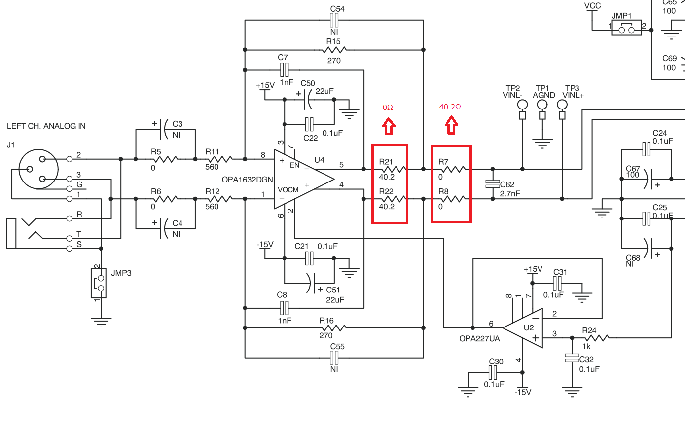
Could you please give me your advice regarding the following stabilization regsistors of R21 and R22 ?

Q1. Optimum value of stabilization resistance
It seems that the resistors(40.2Ω) of R21 and R22 are added to stabilize the feedback loop.
So, could you please tell me how to optimize the value for them ?

Q2. Optimum value of isolation resistance
The resistors of R21 and R22 become the isolator if swapping R21 and R22 with R7 and R8 as below.
I also consider the feedback loop is stable.
So, is OPA1632 able to be applied how to use mentioned above ?

Best regards,
Kato

  • Hi Kato,

    You are correct, those resistors are there to stabilize the feedback loop. This is a technique called Riso + Dual Feedback. I have compiled a short presentation to help walk you through the design process for this type of compensation. Please note that the method presented is based on rules of thumb that tend to yield good phase margin and keep the designer away from dangerous territory.

    I noticed  that the design you posted above is from the datasheet for the OPA1632. If you simulate this design you will find it yields a phase margin of approximately 94 degrees. If this is the design you are intending to use I think you will find it quite difficult to optimize it any further (at least in terms of phase margin) and at most you may be able to yield an extra degree or two of margin. 

    1513.Stability Ref Slide.pptx

    Regards,

    Zak Kaye

    Precision Amplifiers Applications

  • Hi Zak-san,

    Thank you for your quick response.

    I cannot simulate the phase margin regarding "Riso + Dual Feedback(Q1)" and "the isolation resistor for the load capacitance(Q2)" since OPA1632 spice model isn't provided to us.
    So, could you please verify it for the above two schematics and give me the results ?
    The above schematic which I mentioned is described in the user's guide of PCM4222EVM.

    Best regards,
    Kato

  • Kato-san,

    I have attached an updated copy of the presentation with the simulations for these two designs added at the end. I also included the simulation files so you can use the models if you'd like to play with the design or look at the transient response. You will notice that the AC transfer characteristics of the two designs looks identical.

    The main advantage of the dual feedback method is that it eliminates the error associated with the voltage drop across Riso. However, Dual feedback circuits will typically take longer to settle for the same Riso and CLoad values.

    2086.Stability Ref Slide.pptx

    Regards,

    -Zak Kaye

    Precision Amplifiers Applications

  • Hi Zak-san,

    Thank you for your special support.

    I understood that the phase margin for "Riso + Dual Feedback" is almost same with one for "Riso".
    By the way, is my understanding correct that the C2 capacitance(4pF) is the input capacitance with the negative input voltage pin ?
    Sorry for overlooking that there is TINA-TI reference design in TI website.
    Then, I will verify the phase margin and the settling time by using it.

    I greatly appreciate your cooperation.

    Best regards,
    Kato

  • Hey Kato-san,

    You are correct, that capacitance represents the input capacitance on the negative pin. It is necessary to add that capacitance because breaking the feedback loop at the inverting pin neglects the interaction the feedback components may have with the input capacitance of the opamp. Let me know if you have any more questions!

    Best,
    -Zak Kaye
    Precision Amplifiers Applications
  • Hi Zak-san,

    Thank you for your special support.

    I understood about the C2 capacitance(4pF), however I have an additional question.
    Is my understanding correct that the load capacitance should be a half of 2.7nF(C3) if simplifying the schematic to a single sided representation for the full differential amplifier ?
    Please give me your advice if I have any misunderstanding.

    Best regards,
    Kato

  • Kato-san,

    Actually, you want to do the opposite. You are cutting the load impedance in half when you simplify to a single sided representation, but remember the impedance of a capacitor is inversely proportional to the capacitance. Therefore, you need to double the capacitance value.

    Regards,

    Zak Kaye

    Precision Amplifiers Applications

  • Hi Zak-san,

    Thank you for your quick response.
    I understood.

    Best regards,
    Kato