Hi,
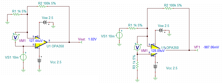
Our customer has made a test of OPA2350 to see the influence of common-mode voltage and the input offset voltage caused by CMRR. And the inverting and non-inverting configuration are shown in TINA, as below. However, there are a few problems. And we really appreciate your help.opa2350 inverting.TSCopa2350 noninverting.TSC
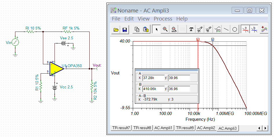
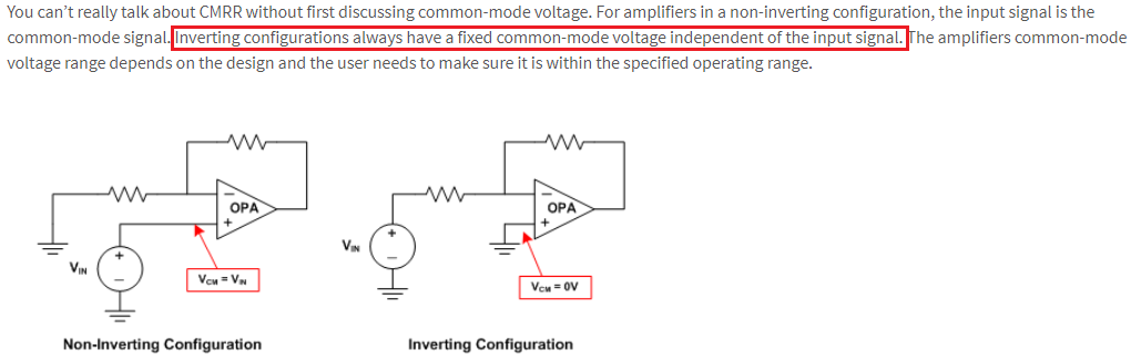
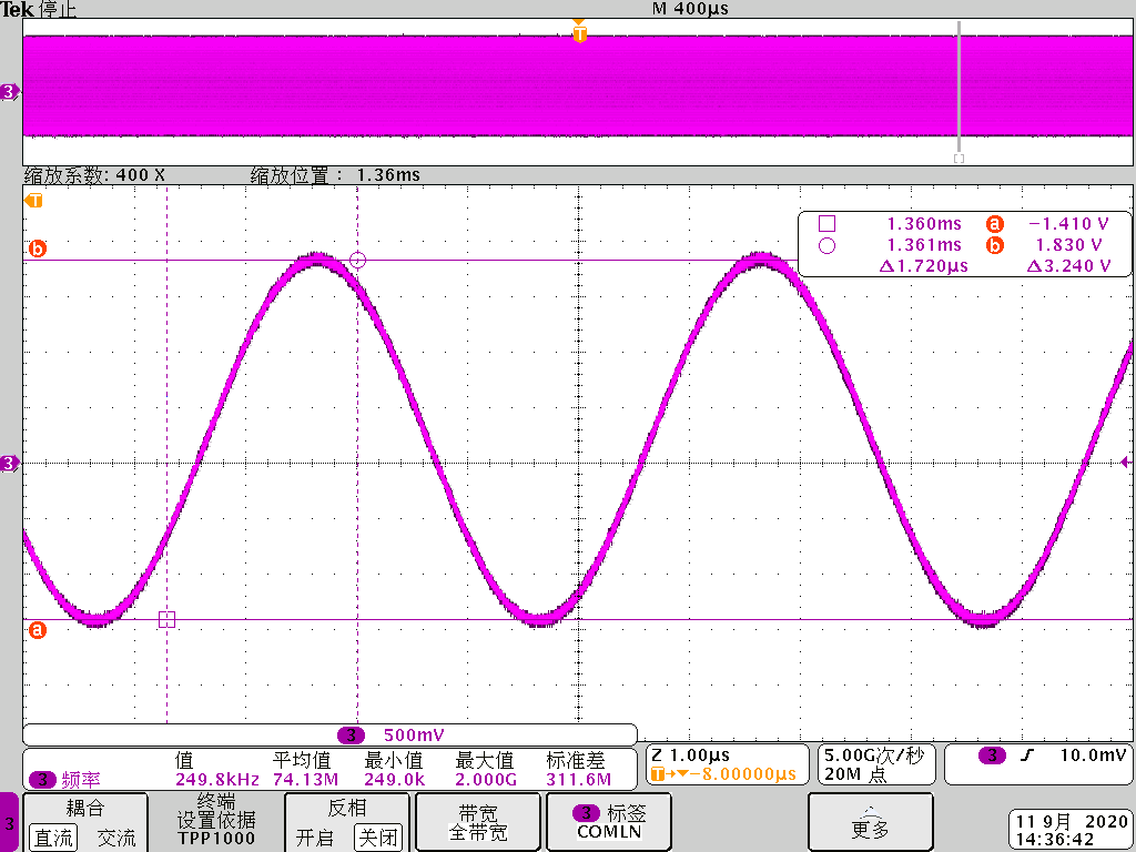
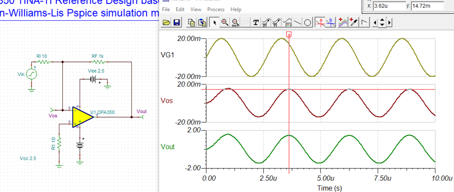
1. In non-inverting configuration, the input signal is 40mV Vpp sinusoidal signal, frequency is 250kHz and 380 kHz. The output signal is shown as below, respectively.
- Why can not the amplifier output get to ±2V?
- And why the output of 250kHz and 380kHz are different? Is it because of the ΔVos caused by CMRR?


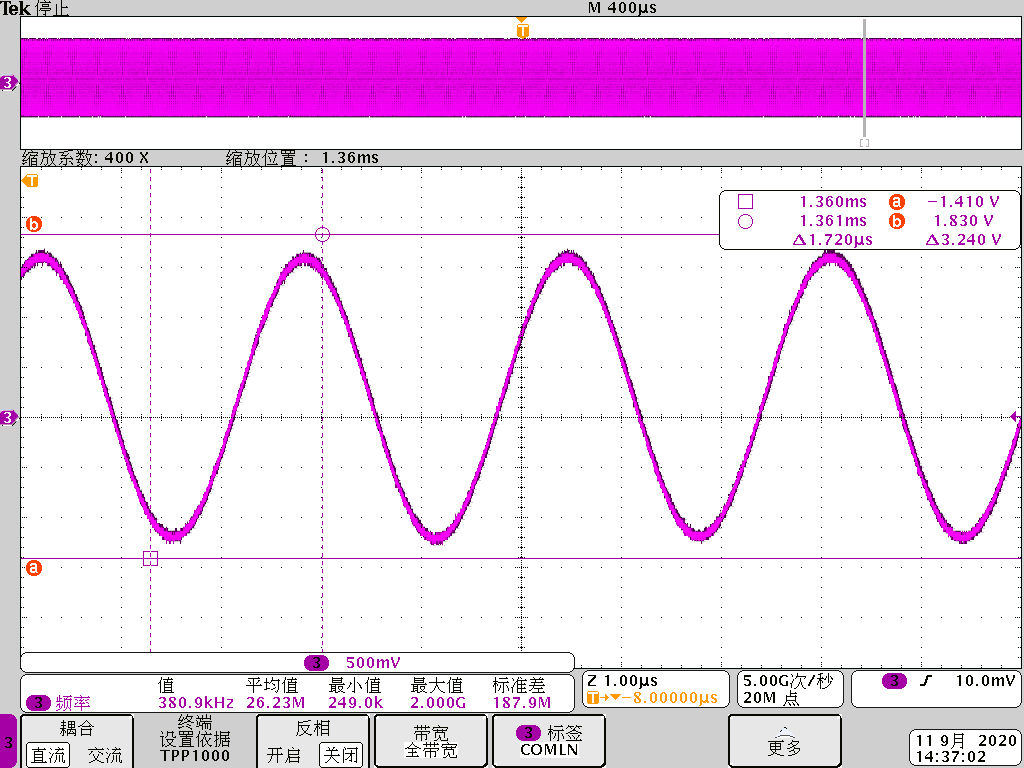
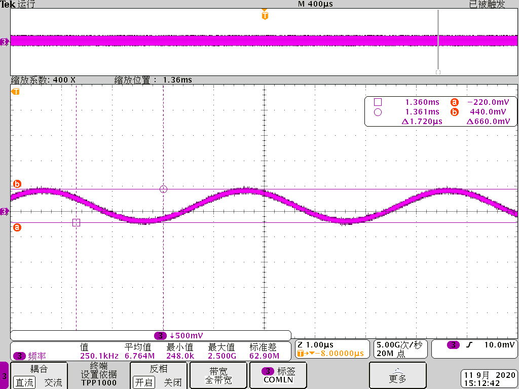
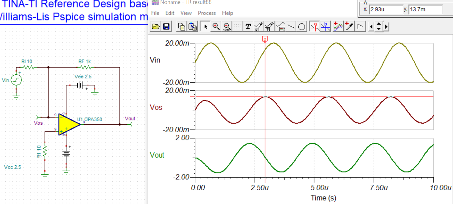
2. In inverting configuration, the input signal is also 40mV Vpp sinusoidal signal, frequency is 250kHz and 380 kHz. But the output signal is shown as below, respectively.
- Why the output is so much lower than ±2V?
- And this time the output of 250kHz and 380kHz are the same. Is it because that inverting configuration doesn't have common-mode voltage?

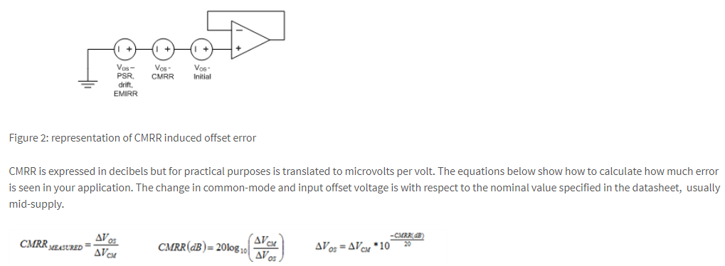
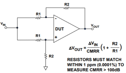
3. Is the equation below correct? Or it should be CMRR=ΔVcm/ΔVos ?

4. About CMRR, we have a question. Since CMRR is common-mode rejection, and in non-inverting configuration, the input voltage is common-mode voltage. Does it mean that the input voltage is suppressed in non-inverting configuration?
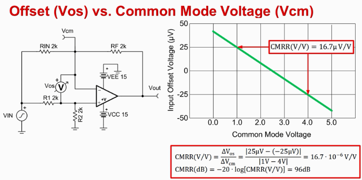
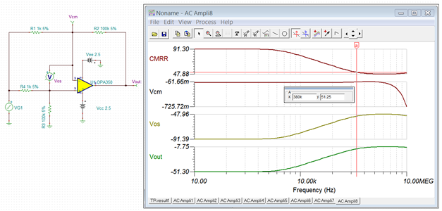
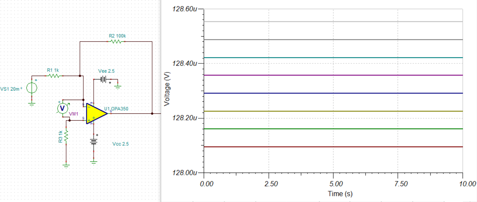
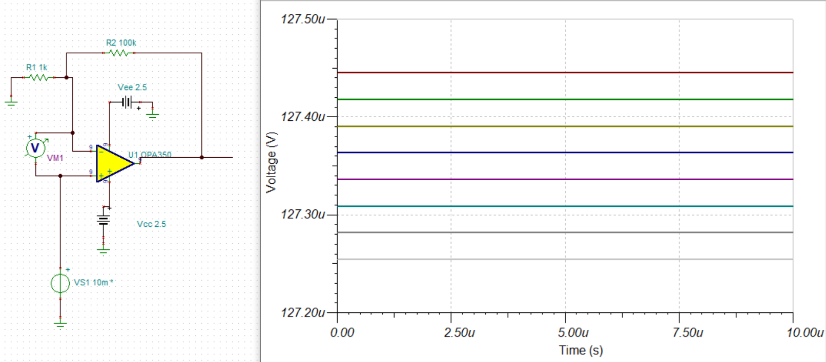
5. Using the equation below, I can calculate that in non-inverting configuration, ΔVos=20mV*10^(-52/20)=0.05 mV. But the peak value of simulation result is about 14.72 mV. Besides, in inverting configuration, ΔVos is not zero. So we got confusion here.
Thank you so much for your support and look forward to your reply.
Best regards,
Wendy