This thread has been locked.

If you have a related question, please click the "Ask a related question" button in the top right corner. The newly created question will be automatically linked to this question.

Asking about charge amplifier

Part Number: TLV2771
Other Parts Discussed in Thread: TINA-TI

Hello everyone, I'm having a school project which is relevant to the piezo sensor. When I read the 'Signal Conditioning for Piezo Sensor", I have some confusing problem that hopes everyone can help my to solve.

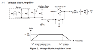
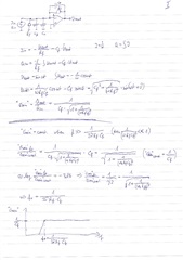
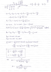
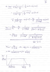
I do not understand why the bandwidth frequency response of those circuits. For Figure 2, I do not how the feedback capacitor and resistor at this point form a low-pass filter that makes the higher cutoff frequency. 
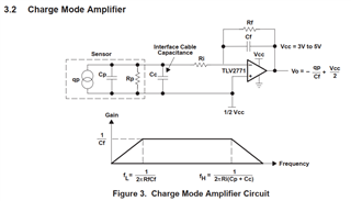
I also do not understand how we get the bandwidth of the figure 3 circuit. 
I'm just a newbie so I hope someone can help me to answer. I very much appreciate each contributed comment

Thank you a lot. 

Sincerely. 

  • Hello Phuc, 

    Can you link the document these images are from?

    All the best,
    Carolina

  • Dear Carolina
    This is the document I mentioned https://www.ti.com/lit/pdf/sloa033

    Hope to see your reply 
    Best regard

  • Hi Phuc,

    Checked the app note. The author (Jim) anticipating the challenge actually explains how to go about it on the appendix. I quickly gave it a swag without reading actually what he explains (maybe I should :)) but I think the key is to remember that the signal here is not i(t) but q(t). q(t) is the integral of i(t), hence in Laplace Q(s)=I(s)/s. 

    So, an "easy" way (not sure if super orthodox one), is to do the analysis with I(s) but in the end, switch the I(s) to sQ(s). The Bode plots are respect to Q(s).

    The other thing to take into account is the usual value of the components on those circuits. With the input parallel parasitic resistors usually being in the order of GOhms or more, the series input resistor Ri being very small, the Rf being MOhms or less (although sure, some specialty circuits may push this to GOhms), and Cf being usually on the order or larger than the parasitic input capacitors.

    With that in mind, for the first circuit, the current gets first multiplied by the parallel impedances (Cp, Rp...). With those caps to ground, that is a LPF with pretty low frequency (large resistors). That voltage then gets amplified by the non-inverting amp, which is also a LPF. But that would be the response for I(s) input. Switch that to sQ(s). That s now multiplies the whole response, making the lowest frequency pole (which is the first of the two as Rp and Rb are very large) "look like a HPF".

    For the second circuit, only the portion of the I(s) current flowing into Ri will get multiplied by the TIA feedback. That first current divider does seem like a LPF again, but the small Ri sets it pretty high. The second LPF is the one created by the feedback network of the TIA. Notice that with standard values, the Rf will be much larger than Ri, so, that sets that pole lower, this time, than the input parasitic network pole. Once again, multiply that by s (from the I(s)=sQ(s)), and you are left with the bottom pole looking like a HPF.

    Hope that helps!
    Eduardo 

  • Hi Eduardo.

    From your explanation, I'm not sure that I can fully understand all the stuff, I guess maybe about 30%. CrySweat smile

    I'm learning this project by myself. So I very thankful if you can help me to write down the explanation in the math formula form so i can easily follow your description.

     Appriciate all the help from you. 

    Thanks for spending your time

    Phuc Pham

  • Hey Phuc, 

    Is there a reason you need an entire formula proof? 
    To better understand the circuit, I would try running a simulation in TINA-TI. 

    All the best,
    Carolina 

  • Hi Carolina.

    My professor asks me to prove it as the bonus mark. Moreover, asGrin an amateur, there are lots of thing I need to learn so I want to understand fully a problem for further applications. 

    I use the Proteus for simulation, but the result doesn't satisfy the formula. I guess I will try TINA - TI. 

    Thank you for your suggestion and advices. 

    Best regards

    Phuc Pham

    Blush

  • Hi Kai.

    Thank you for your recommendation, I have understood the formula to calculate the transfer function of both of them. I just don't know how to get the lower and higher cut off frequency. 

    However, I appreciate your support. 

    Best regards. 

    Phuc Pham 

  • Hey Phuc, 

    The analog engineer's pocket reference design paired with Eduardo's explanation/explanation provided in the article should help you get the mathematical proof. Additionally I would check out the 3V accelerometer app note referenced in the design, it would appear there is a hand analysis already done for you. 

    All the best,
    Carolina

  • Hi Carolina

    Thanks a lot for your recommendations, I'll use those documents for the research.

    Appriciate your support.

    Best regards

    Phuc Pham 

  • Hi Phuc,

    as I already mentioned, application note "sloa033" contains some mistakes and deserves a revision. The major issue is that figure 3 does not show a typcial charge mode amplifier but a variant which is not often used because of the drawback introduced by the sheer existence of Ri:

    When Ri is low a high pass filter with very high corner frequency is created. When Ri is high, on the other hand, Ri creates an enormeous and entirely unnecessary extra noise. But the main disadvantage is that a non-vanishing Ri isolates the sensor from the zero Ohm input of inverting amplifier and as the sensor no longer drives into virtual ground the sensor signal becomes sensitive to cable capacitance and stray capacitance effects.

    I get the following formulas:

    Oops, no way to upload pictures at this place Frowning2

    See here for the maths:

    https://e2e.ti.com/support/amplifiers/f/amplifiers-forum/989838/tlv2771-issues-arround-sloa033a

    Kai

  • Hi Kai. 

    Thank you for your formula Kai. I appreciate it a lot Relieved
    Yeah, when I search other source which mention about the charge amplifier for piezo, I don't see them include the Ri into the schematic. I will make an experiment to test the and review the schematic. 
    I also feel that the sloa033 contains some thing wrong, now I feel relax for your support. 

    Your formula is very specific and easy to follow. 
    Best regards. 

    Phuc Pham

  • Hi Phuc,

    there is a similar appnote from ST.com which also discusses this fake charge amplifier including Ri. This appnote also includes a calculation mistake as it calcalutes the high pass filter corner frequency by only taking Rp into consideration but not Ri. They forget that Ri sees virtual ground and by this is connected in parallel to Rp.

    It's true that the fake charge amplifier (including Ri) can be used in simple circuits which only want to detect whether a piezo is hit or not. Then a high high pass corner frequency can even be helpful and the noise contribution of Ri might not play a siginificant role.

    But that's not what we are thinking about when we talk about the true charge amplifier in a precision application. Then we want the sensor be directly connected to the virtual ground of an inverting amplifier to be able to avoid signal dampening by the cable capacitance and stray capacitance. But this will only work when there's no Ri mounted in the circuit Relaxed

    Kai 

  • Hi Kai
    Thanks a lot. For a beginner like me, this helps me a lot.Relieved 
    Can you please recommend me some good book about integrated circuit which contain math formula with detail solution. I'd love to learn more about it. 

    Thanks a lot. 

    Best regards. 

    Phuc Pham.

  • Part Number: TLV2771

    This is an answer to this thread:

    https://e2e.ti.com/support/amplifiers/f/amplifiers-forum/986054/asking-about-charge-amplifier

    Hi Phuc,

    as I already mentioned, application note "sloa033" contains some mistakes and deserves a revision. The major issue is that figure 3 does not show the typical charge mode amplifier but a variant which is not often used because of the drawbacks introduced by the sheer existence of Ri:

    When Ri is low a high pass filter with very high corner frequency is created. When Ri is high, on the other hand, Ri creates an enormeous and entirely unnecessary extra noise. But the main disadvantage is that a non-vanishing Ri isolates the sensor from the zero Ohm input of inverting amplifier and as the sensor no longer drives into virtual ground the sensor signal becomes sensitive to cable capacitance and stray capacitance effects again.

    I get the following formulas (first for the true charge amplifier without Ri (I), then for the variant including Ri (II and III):

    Kai

  • Kai,

    Would you like this thread to be joined with the referenced thread?

  • Hi Ron,

    yes, this would be a good idea.

    Kai