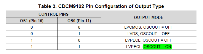
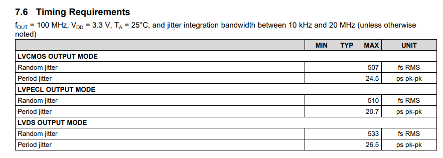
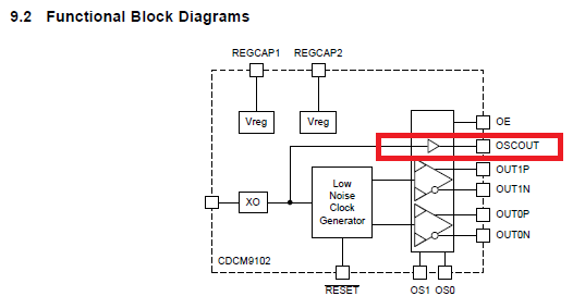
When OS1=1 and OS2=2, OSCOUT is enabled in LVPECL mode. In this case, what is the performance (Duty, Jiter and so on) of the clock signal from OSCOUT pin?
Thanks
Tamio
When OS1=1 and OS2=2, OSCOUT is enabled in LVPECL mode. In this case, what is the performance (Duty, Jiter and so on) of the clock signal from OSCOUT pin?
Thanks
Tamio