A related question is a question created from another question. When the related question is created, it will be automatically linked to the original question.
If you have a related question, please click the "Ask a related question" button in the top right corner. The newly created question will be automatically linked to this question.
LMX2595: There is a fixed 20us no frequency output time when frequency switching
When you switch to 100MHz, did you program the following registers in sequence?
1. R45 to set OUTA_MUX to "channel divider"
2. R75 to set the CHDIV value (ps: div/11 is not a valid value, only even numbers are supported)
3. R36 to set the PLL_N value
4. R43 and R42 to set the PLL_NUM value
5. R0 to trigger VCO calibration
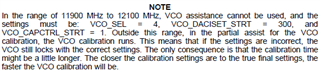
The programming sequence is fine. If you have OUT_FORCE = 0 and OUT_MUTE = 1, when you use the CS# signal of R0 to trigger the test equipment, there will be no output for some time while the VCO is being calibrated. Since you are using close frequency assist, depending on the existing and new VCO frequency, the calibration time could vary a lot. If both frequencies are very close and within the same VCO core, the calibration time will be very short.
However, if you were switching the output frequency from 50MHz to 100MHz, all you need to program is CHDIV. A VCO calibration is not required.
Hello Fung, I haven't received your reply for a long time. I'm a little worried about you. I program the register order you sent me. I use the close frequency assist recently,and I test it that OUT_FORCE = 1 and OUT_MUTE =0, or OUT_FORCE = 0 and OUT_MUTE =0.The No frequency output time is still 20ms. It's so strange.
Is the problem happen when the VCO frequency falls into below zone?
I can't remember the behavior of close frequency assist, but with auto-calibration, if you have OUT_FORCE = 0 and OUT_MUTE = 1, the output will not mute during calibration.
Let's try an experiment, run the following configuration to make the VCO lock to 11000MHz with auto-calibration. Then program PLL_N to 551 and then program R0 to trigger auto-vco calibration.
Next, repeat the above experiment but make QUICK_RECAL_EN = 1 before programming PLL_N to 551. Will the output be muted?
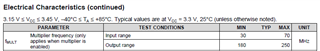
BTW, there are min. input frequency and max. output frequency requirement to the MULT, we cannot get 50MHz fpd from a 10MHz reference.
I am sorry, it was a typo, the output will not mute when OUT_FORCE = 1 and OUT_MUTE = 0.
Did you mean, you got the output muted with both auto-calibration and quick_recal_en=1 ? if this is true, I will have to ask my colleague to verify this.
The MULT frequency requirement is specified in the datasheet.
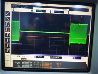
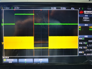
Does the green trace refer to my reply on June 22? That line is the trigger signal for writing the R0 register,Pull up before writing R0 and pull down after writing. such as in my code TP_ H is Pull up, TP_ L is Drop down.
Yellow is the output frequency. In the oscilloscope window, each grid is 10us, and there is no frequency in the middle. The time of two grids is just 20us.