A related question is a question created from another question. When the related question is created, it will be automatically linked to the original question.
If you have a related question, please click the "Ask a related question" button in the top right corner. The newly created question will be automatically linked to this question.
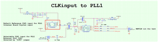
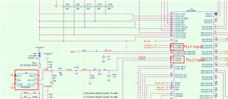
LMK04828: the relationship between the input clocks of PLL1 and PLL2
10MHz is a common standard reference signal across many pieces of test and measurement equipment, so it is helpful to provide the ability to lock frequency of the LMK04828 on the board with other equipment such as signal generators, frequency counters, spectrum analyzers, etc.
I don't think the answer above does a good job of explaining why this system-level design decision occurs commonly across many pieces of test and measurement equipment, so I will also try to explain this design decision as well. There are typically two reasons why someone might choose to use a dual-loop jitter cleaner:
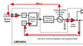
The frequency of the input does not align well with the frequency of the output. For example, 10MHz in (due to OCXO limitations or system-level spec on reference input choice), 2457.6MHz out... the greatest common divisor of 10MHz and 2457.6MHz is 400kHz, which would severely limit the phase detector frequency and the loop bandwidth, and would greatly impact the clock jitter on a single PLL. Instead, we can use an intermediary stage (PLL1) with a low-noise VCXO, to utilize a low phase detector frequency and a low loop bandwidth effectively while translating the frequency of the VCXO to a more favorable domain for the high-frequency PLL (PLL2). In this case, a common choice would be a 122.88MHz VCXO with a 10MHz reference at PLL1, allowing PLL2 phase detector to go up to 122.88MHz (almost 3 orders of magnitude higher) and improve in-band noise by over 15dB, at a much higher loop bandwidth.
The choice of low-frequency reference usually comes from a few different possible places:
A common OCXO model or frequency
A recovered clock frequency that cannot be very high due to recovery loop limitations
A requirement to transmit the signal across very long distance with low loss (higher frequencies are attenuated more by longer cable runs) or to multiple targets on the same PCB (lower cost for low-skew reproduction in a buffer)
The input clock is noisy, and the choice of reference input frequency is arbitrary since it is substituted by a VCXO anyway. You might see a 100MHz reference and a 100MHz VCXO used for PLL1 of a jitter cleaner architecture with low loop bandwidth, when the 100MHz reference clock is noisy or recovered and has poor noise above PLL1 loop bandwidth. This is more common in wireless applications where the clock frequency is often recovered from data signals.
Changing the input frequency to the PLL may or may not have an effect. If you changed the reference input from 10MHz to 100MHz, but the phase detector remained the same frequency, nothing would change. On the other hand, if you changed the phase detector frequency to accommodate the higher possible range with a 100MHz reference, this would alter the loop gain and the stability. We have a calculation tool, PLLatinum Sim, which allows you to examine the effect of these changes yourself.
I will also point out our TI Precision Labs training series which goes over the fundamental aspects of PLL design and system implications in great detail.
You could just use the 100MHz VCXO, but the frequency of the VCXO will be 100MHz + ε, where ε is some small error relative to absolute 100MHz due to temperature drift or control voltage tuning range. If you tried to measure the PLL output frequency with a frequency counter or some other instrument that was specified as "perfect" 100MHz (at least for the purposes of comparison), there would be some difference ε * Fout/100MHz in the measured output frequency due to the error from the VCXO.
Recall that most instruments include a 10MHz reference on-board, and this reference can be brought out of the instrument or another instrument's 10MHz can instead be connected to override the on-board 10MHz. This is an industry-standard synchronization mechanism between different instruments which must work with frequency, such as frequency counters, spectrum analyzers, oscilloscopes, etc.
By including PLL1, we can take the built-in 10MHz reference oscillator output on the frequency counter or other instrument and provide it as a reference into LMK04828 PLL1, which eliminates the measurement error. Alternately, we can buffer a copy of the on-board 10MHz reference, and connect the buffered copy to the 10MHz reference oscillator input on the frequency counter. Then, by locking the VCXO to the 10MHz reference on the PCB, the error from the 10MHz reference would be common for both the PLL and the frequency counter. We could take the 10MHz directly to PLL2 and omit the VCXO and PLL1, but the phase detector frequency would be an order of magnitude lower and the PLL performance would be 10dB worse in-band. We have no way to lock the VCXO to an external reference without PLL1. We could add a buffer/divider to divide-by-10 and transmit the VCXO reference off-board to our instruments, and simultaneously provide 100MHz to PLL2... but this requires a lot of extra devices, and still gives us no way to lock the VCXO to an external instrument's 10MHz reference.
It is worth noting that usually the 10MHz reference has very good close-in noise (maybe up to 1kHz) but sometimes the instrument's 10MHz reference has a very high noise floor compared to a VCXO. So PLL1 still frequently behaves as a jitter cleaner in this scenario, even while locking a VCXO to an external reference and increasing the phase detector frequency at PLL2.
While we don't have anything comprehensive, we do have default configurations that show final/working register state, and TICS Pro has some features (set modes page, SYNC/SYSREF procedure declarations) which can simplify some aspects of the configuration process.
To your point, a flowchart or a decision tree could improve usability. I'll make a note of this for future datasheets.
Thank you very much, I will try to use the TICS Pro.
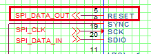
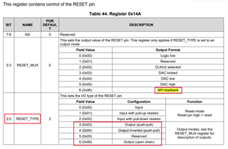
Another question, I want to configure the RESET pin of LMK04828 as the SPI data out pin(Figure 1), but I don't know choose which output mode(Figure 2).
Output (push-pull) works like a standard CMOS output driver, logic high = 3.3V and logic low = 0V. Output inverted (push-pull) is the same thing, but inverted: logic high = 0V, logic low = 3.3V.
Output (open-drain) assumes an external pull-up resistor is used. Open-drain makes the most sense when the I/O returned to the microcontroller/FPGA/etc. utilizes 2.5V or 1.8V I/O, since the pull-up resistor can be connected to the programmer I/O supply instead of the device internal 3.3V rail for logic high signals. Open-drain is also useful if the readback bus must be shared with another device.
Yes, this is a mistake in the datasheet. There are three registers corresponding to the SPI_LOCK field which set the 13th bit to access. I'll put it on the list of things to fix in the next revision.
1) If I use push-pull, may I debug this signal by ILA Core in FPGA?
Yes, this should be possible. I'm not totally sure how the ILA core is implemented, but it should have the ability to monitor any signals on the I/O once they get latched into the FPGA registers somewhere.
As long as one of the GPIO is configured as SPI readback, SPI 4-wire mode will be active. Note that technically it is possible to use 3-wire and 4-wire mode simultaneously; if you want to use 4-wire mode and also disable 3-wire mode, make sure SPI_3WIRE_DIS=1 (this should be the default).