This thread has been locked.

If you have a related question, please click the "Ask a related question" button in the top right corner. The newly created question will be automatically linked to this question.

LMK04828: Impedance matching questions

Part Number: LMK04828
Other Parts Discussed in Thread: ADS42JB46EVM, LMK04832, CDCLVP111-SP, LMK03328, ADS42JB46

Hi everyone,

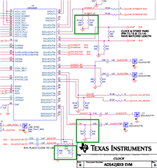
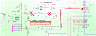
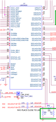
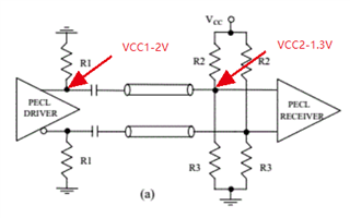
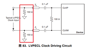
1) I don't know why there are 3 kinds "impedance matching" in the design schematic of LMK04828 (in ADS42JB46EVM) because I think the Clock-output pins are same.

2) How should I choose the resistance size for impedance matching, because I don't know the characteristic impedance of the transmit line.

Thanks for all replies.

  • Hi Nan,

    1. The components in the green boxes are emitter resistor biasing for LVPECL output stages, and are not termination. Since it is impractical to terminate LVPECL to VCC-2V through 50Ω, by convention we use an emitter resistor close to the device pins to control the necessary bias currents in the driver stage - in effect we are "emulating" the VCC-2V component of the load. These emitter resistor biasing components are typically 120Ω for AC-coupling to 50Ω single-ended loads, or 240Ω for DC-coupling to 100Ω differential load. There are also 560Ω resistor footprints on some outputs, due to a note in the datasheet about LVDS startup requirements.
    2. Characteristic impedance should be 50Ω. Keep in mind that by placing the emitter biasing close to the source pins, the impact of these components on the overall signal integrity will not be very large; meanwhile, the transmission line and the load will appear as 50Ω single-ended, which is how the driver is simulated and designed to operate.

    Regards,

    Derek Payne

  • Hi Derek,

    Thank you for your all three answers, but maybe I need some time to understand them.

    Thanks again and regards,

    Nan

  • Hi Derek,

    I also have some other questions I don't know,

    1)  Now I want to use a 10MHz Oscillator( SiT9121 in Figure 1), as the input clock of LMK04828, can I configure my output of this oscillator as ADS42JB46EVM shows in figure 2? It's also the something about "impedance matching"? I'm a freshman, not quite understand.

    2)  I found the 100MHz VCXO create one pair differential clock signals but only use one of them as the input of LMK04828 (OSCIN), so why,,, what's wrong with differential signals input?

  • Hi Nan,

    1. The oscillator on ADS42JB46EVM is LVCMOS, and LVCMOS signals have a tendency to overshoot or undershoot when driven straight into capacitive loads. That overshoot and undershoot can introduce undesirable harmonics and radiate energy, so it is common for designers to slightly attenuate the output of the LVCMOS stage using a small series resistor. 22Ω to 33Ω range is common, and along with load capacitance ~10pF usually forms a small RC filter in the 500MHz to 1GHz range to roll off higher order harmonics that can contribute to overshoot/undershoot.

      SiT9121 is differential LVPECL/LVDS. The LVPECL variant would require emitter resistors to ground, and I'm not sure the EVM has support for LVPECL emitter resistors to GND (I am not sure where to access the schematics). The LVDS variant would require 100Ω differential termination at the clock input, and I'm also unsure if the EVM has support for this, but my guess is that this is already present. I don't think they would need the series resistors shown with the LVCMOS signal path in Figure 2.
    2. The VCXO has 6-pin and 4-pin variants that share the same package size. Pins 2 and 5 would not be present on the 4-pin package, but other pins would be in the same positions. It is possible that the ADS42JB46EVM has the 4-pin device on the 6-pin footprint, and leaves the pin5 components unpopulated since there is no output from the VCXO on that path. The 6-pin footprint would then be provided for compatibility with other VCXOs from the same manufacturer. Differential input is supported by LMK04828 on all clock inputs including OSCin.

    Regards,

    Derek Payne

  • Hi Derek,

    Thank you very much,

    About question 1, I maybe need some other time to understand, but I have get what I want I think. So what you mean that may I don't need to use load capacitance ~10pF because SiT9121 is differential LVPECL/LVDS but not LVCMOS?

    About question 2, what you mean is it's just the VCXO, on ADS42JB46EVM, which has 4 pins, but the footprint has 6 pins, so if I choose a 6 pins VCXO (with differential output) to replace the 4 pins part, it works too, right?

    Thanks again,

    Nan

  • Nan,

    For question 1, the load capacitance is usually the pin capacitance of whatever is receiving the signal, whether it is LVCMOS, LVPECL, or LVDS. Normally there is no need or reason to add additional load capacitance to the receiver outside of the pre-existing pin capacitance, since the same effect can be accomplished by adding a series resistor, along with the added benefit that a series resistor placed near the load can help reduce the impact of reflections. And it only really makes sense to add series resistance to LVCMOS. LVDS is current controlled to produce specific levels at the receiver across 100Ω termination. LVPECL output structure is designed to operate cleanly across a wide range of transmission line lengths, into 50Ω single-ended termination on each leg of the differential pair (or 100Ω differential, with some emitter resistor tweaks as mentioned previously). 

    Key point: most LVCMOS drivers are not designed for 50Ω impedance load. When the output stage is a push-pull structure with FETs to VCC/GND, it is very difficult to control the impedance of both FETs to be 50Ω source and sink at all times, since the impedance of the FET will change as a function of the voltage across it. So LVCMOS is only really used for low-frequency clocks or short runs of higher frequency clocks, along with techniques like series resistors to reduce ringing, because it is not capable of operating at higher frequencies without significant signal quality degradation, additional reflections, and lost harmonics at higher frequencies.

    So, you do not need any extra load capacitances, the pin capacitance of your receivers will already load the outputs of your driver. Series resistor for LVCMOS is just to help with reflections on an output stage that fundamentally cannot have well-controlled output impedance. LVPECL and LVDS have good control of the output impedance across frequency, so they typically don't need or want series resistors in the signal path before termination.

    For question 2. you have understood me correctly. A 4-pin device like Crystek CVHD-950 or a 6-pin device like Crystek CVPD-922 could both be used with the 6-pin footprint equally well; you'd just populate additional components in the path to OSCIN_P for the 6-pin device.

    Regards,

    Derek Payne

  • Hi Derek, In ADS42JB46EVM schematic, the DCLKOUT12P/N are also defferential pairs, maybe 240 OHM to match impedance if the out clock is LVPECL mode, but why 120 OHM?

  • Nan,

    To make a long story short, 120Ω achieves the swing values closest to the datasheet in AC-coupled LVPECL output, but 240Ω AC-coupled is often sufficient and significantly reduces current consumption. See https://e2e.ti.com/support/clock-timing-group/clock-and-timing/f/clock-timing-forum/759686/lmk04828-proper-emitter-resistor-for-lvpecl-output

    DC-coupled with 240Ω emitter bias resistors also tends to work best to achieve the same swing and VOH/VOL as the datasheet. If you do the math, you will find that this configuration actually has the output pins sinking current; in practice, the actual circuit design within the output driver stage is not usually just a transistor emitter, as the multimode output driver must support other push-pull style architectures like LVDS or HSDS, so sinking current with the output levels set to LVPECL can still be possible.

    Regards,

    Derek Payne

  • Hi Derek,

    I find something about "emitter resistor biasing for LVPECL", which means that the emitter resistor for LVPECL output is about 143 ohm to 200 ohm to make sure that output common mode voltage is about VCC-1.3V and impedance 50 ohm but not VCC-2V? 

    Am I wrong? Maybe I do not express clearly...

    Regards,

    Nan 

  • Nan,

    Depends which device is used and what the output driver specs are. Different manufacturers or even different teams within the same manufacturer can produce different LVPECL implementations. There are also I/O standards for 2.5V LVPECL outputs, for which VCC - 1.3V approximately centers the output common mode. For virtually all TI clocking devices, Including LMK04828 and LMK04832, LVPECL with 120Ω emitter resistor to GND gives the appropriate AC-coupled swing for 3.3V LVPECL, and 240Ω to GND gives appropriate common mode and swing for DC-coupled 3.3V LVPECL. There's a few devices like LMK03328 or CDCLVP111-SP which behave differently due to different I/O levels or alternate (and very old) supply biasing schemes. And of course other manufacturer's LVPECL implementations may differ.

    Regards,

    Derek Payne

  • Hi Derek,

    Thank you very much! So if I use one 3.3V standard LVPECL(VCC1-2V) mode driver device, and another 2.5V standard LVPECL(VCC2-1.3V) device as receiver, what I need to do is use different emitter bias resistors to make sure appropriate common mode voltage, right?

    Where VCC1 is 3.3V, VCC2 is 2.5V

    Like below figure :

  • Nan,

    R2/R3 are important if the PECL receiver is not self-biasing. Many modern receivers implement R2/R3 combination inside the input stage of the IC for convenience, or implement some kind of "universal" input receiver which can accept many different input formats. You usually need to check the input signal requirements given in the receiver datasheet.

    In AC-coupled LVPECL output, the R1 emitter resistor to GND can be selected purely to give the appropriate signal swing, since the capacitor between driver and receiver blocks any common mode differences. Since both 2.5V LVPECL and 3.3V LVPECL standards implement ~800mV VOD, 120Ω emitter resistors for TI LVPECL output stages are still valid.

    In DC-coupled LVPECL output, especially translating from 3.3V to 2.5V I/O standards, or interfacing LVPECL to DC-coupled LVDS, there are a handful of level translation tricks that can be used which will influence the emitter resistor biasing choices. In these cases it is usually more critical to achieve the correct common mode than the full LVPECL amplitude. The slew rate of these DC-coupled level translations can sometimes be degraded because of the reduced amplitude, which can increase the phase noise. Most of the time, it makes more sense to AC-couple LVPECL to a receiver which can accept LVPECL amplitude, and use a different I/O standard when the signal swing is limited such as with LVDS.

    Regards,

    Derek Payne

  • Hi Derek,

    I have seen the datasheet of ADS42JB46, I understand the "universal" input receiver you said, but the recommended bias emitter resistor is 150 ohm, I don't know why, and I don't know the output LVPECL driver configuration inside LMK04828 or receiver inside ADS42JB46, so I can't do the math, thanks.

    Regard,

    Nan

  • Nan,

    You would need to ask the data converters team why they chose 150Ω on their EVM. Most of the time, the data converters team cares less about matching a spec exactly, and more about getting high enough slew rate and signal swing to satisfy their data converter clock requirements. These parameters are heavily process-dependent, and our data converters use a wide range of different processes which can have very different signal swing and amplitude requirements

    In other words, do not get carried away trying to derive the perfect emitter resistor value. I have seen 120Ω, 150Ω, 180Ω and 240Ω all used on TI EVMs without much impact on phase noise performance, regardless of standard compliance, because the input stage of most data converters rarely needs perfect standard-compliant LVPECL.

    Regards,

    Derek Payne