I'd like to use the CDCLVC1310 in a design I'm updating due to part availability. I'm interested in this device due to low additive jitter; a requirement. Also it has LVCMOS outputs; another requirement.
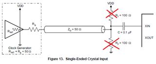
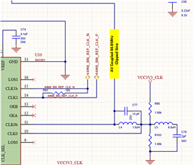
My VCTCXO has a 0.8V, clipped sine wave output. Can I use the XTAL bypass mode and bias this to a level to make the DCDLVC1310 work? Or, would it be better to use one of the legs of and LVDS input, biasing both legs to a common dc level like shown here? This is the circuit I'm reworking.
Thank you,
-j