This thread has been locked.

If you have a related question, please click the "Ask a related question" button in the top right corner. The newly created question will be automatically linked to this question.

LMK04828: Request for schematic review

Part Number: LMK04828
Other Parts Discussed in Thread: ADC32J25EVM

Hello,

I would like to have our schematic reviewed.

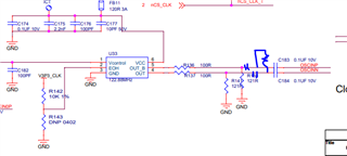
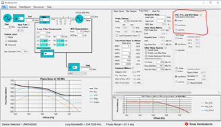
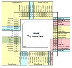
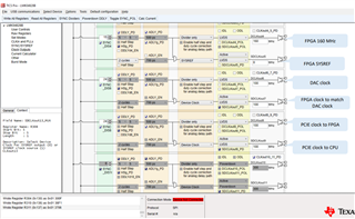
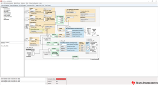
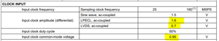
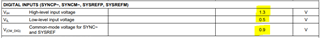
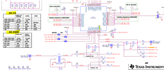
The design includes LMK04828 to support ADC32J25IRGZT and Xilinx FPGA.

Thank you,

Andrew

  • Hello Andrew,

    Could you please attach your schematic so we can help you.

    Thanks,

    Andrea

  • FIBERSENSE_V1P07.pdf

    Hi Andrea,

    The LMK04828 circuit is on Sheet 18.

    • provide clocks to ADC32J25IRGZT on Sheet 15
      • DACCLKP/N: 160 MHz
      • SYSREFP/N: 8 MHz
    • provide JESD204B clocks to FPGA
      • MGTREFCLK0P/N: 3.2 GHz (do we need to provide the line rate for JESD204B?)
      • FPGACLKP/N: 160 MHz

    Questions

    • Is LMK04828 the right fit for the frequency plan?
    • What frequency should I use for the clock input?
    • Once we decide on the frequency plan, I suppose TICS Pro can be used to figure out the various configurations

    Regards,

    Andrew

  • Hello Andrew,

    Because you are trying to output a 3.2 GHz signal from the device, the LMK04828 wont give you enough frequency range to obtain that output. However, the LMK04832 can reach up to 3255 MHz using VCO1 as the internal VCO. From there, you can set divider values of 20 for 160 MHz output frequencies, 400 for 8 MHz SYSREF output frequency and 1 for the 3.2 GHz output frequency. Also, you do not need to provide the line rate, the SYSREF frequencies (given as 8 MHz) is enough.

    Regarding the input frequency, that will depend on your application. What is driving the LMK04828? Different applications have different output frequencies which will be the input to our system. Also, any input frequency can be used while it meets the data sheet specs, if you have no descriptions from the previous devices before the LMK.

    Once you tell me what input frequency you are using, we can go ahead and complete the TICS Pro as you mentioned.

    Thanks,

    Andrea

  • Hi Andrea,

    After reviewing the JESD configuration of the FPGA, the ref clock can be 80, 160, or 320 MHz.  The PLL within the FPGA will bring it up to 3.2 Gbps.  Having said this, could you provide the clocking scheme?  I think we can go ahead with 20 MHz or 32 MHz TCXO.  I would appreciate your help on TICS Pro.

    Regards,

    Andrew

  • Hi Andrew,

    That's correct. Usually for the JESD204B complaint clocks, FPGA requires the low frequencies (FPGA REFCLK / CORECLK in few 100 MHz) and that should be able to generate using the LMK04828. 

    For the integer clocks out frequencies (SYSREF - 8MHz, DACCLKP/N - 160MHz, FPGACLKP/N - 160MHz and MGTREFCLK0P/N - 80/16/320MHz), LMK04828 internal VCO should be LCM of these frequencies and VCO can be selected 2.4GHz. To have better phase noise / jitter performance, phase detector frequency should be higher. Hence need to replace the existing 122.88MHz VCXO with the integer frequency VCXO, say 100MHz / 160MHz.

    Attached is the TICS Pro config file FYR.

    8272.LMK04828.tcs

    Regarding the LMK04828 schematic, please see the feedback below:

    1. Should be follow the supply section guidelines from section 10.6 in datasheet and based on LMK04828EVM user's guide.

    2. OSCin input requires the 100ohm differential termination for LVPECL input signal. Hence, can keep 100ohm before C183/C184 and insert same cap after R138/R141 to isolate the common mode voltage variation.

    3. SYSREFout signals should be from the odd clocks out (SDCLKoutX).

    4. If MGTREFCLK0P and FPGACLKP has the same frequency from DCLKou0 and SDCLKout1, then should be ok, otherwise change these clocks to different DCLKout.

    5. For LVDS output, if the FPGA has internal 100ohm impedance, then need to provide the 560ohm otherwise keep 100ohm.

    6. What are the clock frequency and output format for CLK_TX and CLK_RX? If both are same frequency, then its good else change to other DCLKout.

    Thanks!

    Regards,
    Ajeet Pal

  • Hi Ajeet,

    I have decided to use 40 MHz for the input clock as well as VCXO.  The 40 MHz VCXO decision was driven by the cost, which tends to increase substantially for 80 MHz and above.  In TICS Pro, I was able to generate 2400 MHz VCO.  

    From there I was able to generate the ADC and the DAC clocks as well as 100 MHz used for PCIE.

    The configuration is described in the pdf. 

    The TICS Pro config file is also attached.

    Could you review the filter design, "C1" (C143), "C2" (C144), and "R2" (R121)?

    config_lmk04828.pdf

    40M.LMK04828.tcs

    1. I have reviewed the power supply design and it is consistent with Section 10.6.  For reference, this design is based on my previous development to support JESD204B, which was successful.  
    2. For the 40 MHz VCXO, all VCXOs I could found have a single-ended CMO output.  So I followed Section 10.3.2 (Driving CLKin and OSCin Pins With a Single-Ended Source).  I used the same approach for CLKIN1p.  I am assuming I want to use CLKIN1p vs CLKIN0p as the primary clock source.
    3. SYSREF is now on SDCLKOUT3 (8 MHz).
    4. I updated multiple independent clocks to go to FPGAs.  
    5. I've followed the recommendation of using 560 Ohm on the transmitter side and added 0.1uF on the FPGA side, assuming we will use the 100-Ohm internal termination, which is a valid assumption.
    6. I used DCLKouts for other FPGA clocks.

    Thank you,

    Andrew

    FIBERSENSE_V1P10.pdf

  • Hello Andrew,

    Ajeet should get back to you soon. If not, I'll loop back and help you.

    Thanks,

    Andrea

  • Hi Andrew,

    Your frequency plan looks good and seems you are operating LMK04828 in dual PLL mode with on-board reference (CLKin1) or external reference from CLKin0 (J16). All input reference pins terminations are good.

    With the 40MHz VCXO, you can keep the PLL2 phase detector frequency 80MHz using the doubler in path, which would help to improve the overall phase noise / jitter performance. In the PLLatinum Sim tool, you can import the VCXO data and can simulate alongwith to get the performance including VCXO.


    I am not seeing the SYSREF output for FPGA. Usually for JESD204B complaint clocks, FPGA would also require the SYSREF input. Please ensure from FPGA side and include that too, if needed.

    Thanks!

    Regards,

    Ajeet Pal

  • Hi Ajeet,

    First here are the TICS Pro and PLLatium SIM files.

    I believe they match your recommendations.

    • 80MHz for phase detector
    • Loop filter to match the recommended values
    • Added clocks for FPGA SYSREF and PCIE (to FPGA and CPU). 

    Please let me know if you see any additional issues.

    Regards,

    Andrew

    40M.LMK04828b.tcs

    TICS Pro & PLLatium.pdf

  • Hi Andrew,

    TICS Pro config file looks good, except you can have sync enable to reset the clock dividers to have all outputs aligned/deterministic delay between them. The sync event can be occur once PLL2 locked (SYNC_PLL2_DLD --> 1), keep SYSREF_MUX in "normal sync" mode and SYNC_DISx/SYNC_DISSYSREF --> 0. Once, the divider are reset after locking the PLL2, change SYSREF_MUX in Continuous (Once the JESD link is establish, turnoff the SYSREF to avoid SYSREF spurs at DCLK) and SYNC_DISx/SYNC_DISSYSREF --> 1.

    LMK04828b_updated_SYNC.tcs

    For the noise sensitive clocks, I would suggest to use those clocks from different clock group, which will have less crosstalk between clocks out (like you have ADC clocks from CLK group 1).

    Thanks!

    Regards,
    Ajeet Pal

  • Hi Ajeet,

    Thanks again for the detailed feedback.  I have compared the two TICS Pro config files to understand the differences.  

    I will use your config file when I have the board built.

    As for the Clock Group, incidentally the ADC clocks are in its own Clock Group, Group 1. 

    For our application, the DAC is intended to generate a square wave with the amplitude controlled by the user.  So it is not very noise sensitive.

    Let me know if you see any other issues, the loop filter, input clock circuits, LVDS/LVPECL caps/resistors, ...

    If all look okay, we can close this case for now.

    Regards,

    Andrew

  • I have also noticed you have arrived at 2400 MHz VCO0 slightly different

    N divider is set to 100

    PLL1 phase detector frequency is 0.4 MHz

  • Hi Andrew,

    From the schematic, SDCLKout5 is opened but TICS pro setting shows FPGA SYSREF. You need to update the schematic for FPGA SYSREF out. Similarly for (SDCLKout9) PCIE clock to CPU.

    Regarding the PLL1 phase detector frequency, just modify the R/N dividers for integer frequency. Earlier it was in decimal 0.3333333, anyways it doesn't matter and can be changed during the programming.

    Thanks!

    Regards,

    Ajeet Pal

  • Hi Ajeet,

    My apologies.  

    Here's the updated schematic.

    Could you review?

    Thank you,

    Andrew

    fibersense_v1p15.pdf

  • Hi Andrew,

    For the FPGA clocks, I think all termination looks good and configured for LVDS output.

    Regarding the ADC clock inputs, I believe you should be following/review from ADC side. That means, the LMK04828 should meet the ouptut swing and common mode voltage (for DC coupled).

    ADC32J25EVM schematic:

    Right now, you have configured SYSREF in AC coupled with LVDS but it may not support the amplitude requirements. I think, you should changed the output termination based on EVM schematic and go ahead if AC coupled or DC coupled SYSREF options.

    Thanks!

    Regards,

    Ajeet Pal

  • Hi Ajeet,

    Thanks again for your feedback.

    Please review the updated schematic.

    FIBERSENSE_V1P16.pdf

    Regards,

    Andrew

  • Hi Andrew,

    The schematic looks good.

    Thanks!

    Regards,

    Ajeet Pal

  • Hi Ajeet,

    Thanks again for your support

    I'll let you know once I have tested the board.

    Regards,

    Andrew