This thread has been locked.

If you have a related question, please click the "Ask a related question" button in the top right corner. The newly created question will be automatically linked to this question.

CDC3RL02: Vldo output voltage and latency

Part Number: CDC3RL02

Hi there, 

two questions about the CDC3RL02BYFPR

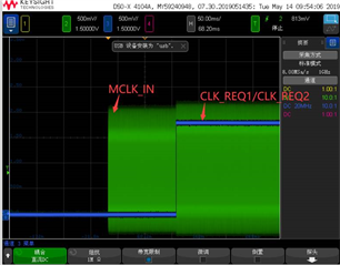
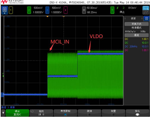
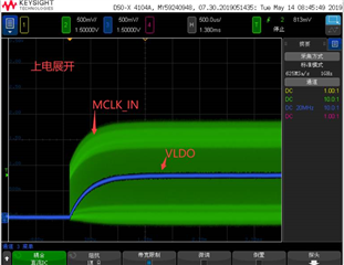
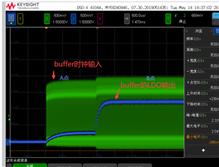
Test condition. the vbatt Is on, MCLK_In is 27Mhz

1. the vldo output is 0.8 when is CLK_REQ is low. The Vldo goes to 0v if MCLK_in is removed.

2. the VLDO output clk has 200 us delay after CLK_REQ is on.

are this two behaviors normal operation?

BRs

Shubiao

  • Hi Shubiao,

    I am happy to assist with your questions. Followings are my inputs to your questions:

    1. I do see that datasheet refers the VLDO output goes to ground when CLK_REQ_X are low in section 9.2. Currently, I am unsure about the relation between MCLK_IN removal to LDO output. I need to find out that from chip designer by looking at internal circuitry. Looking at the block diagram it should go low when there is no CLK_REQ_X since LDO is powered down. 

    2. LDO start up time is about 200 us at VBATT = 2.3 V when a CLK_REQ_X is initiated. This behavior should be normal. Please confirm if you are using the same VBATT conditions.

    Best,


    Asim

  • Thanks Asim,

    for question 1, i would capture some waveform later. 

    BRs,

    Shubiao

  • Hi Shubiao,

    That would be helpful. I would try to reproduce the same results on my end too.


    Best,

    Asim

  • Asim

    please refer to customer my measurements.

    fig1. is MCLK_IN and CLK_REQ

    fig2, is MCLK_IN and LDO ouptut

    as you can see form fig2. the LDO output 0.8V, before CLK_REQ is on .


    zoom in at trigger point. 

  • Hi Shubiao,

    Thanks for the waveforms. Could you confirm specific test condition like VBATT, VLDO pin capacitors etc?  I will reproduce same in our lab and provide feedback if this is expected behavior. Also can you what is clock source use here? are we powering up that source using LDO?

    Best,

    Asim 

  • Hi Asim,

    any update from your side?

    please refer to my sch as below.  VLDO is not used for external circuit. 

    when i change resisters shown in the SCH, the VLDO output is decreased from 0.8V to 0.3V, and the CLK OUT doesn't output signal before the CLK_REQ is on. 

  • Hi Shubiao,

    I have reproduced the same issue as you have seen in our lab. I am waiting for design feedback on internal circuit to understand if there is any relation between MCLK_IN, CLK_REQ and LDO output.

    Chip designer for this part moved to different product line so this might take little more time than expected to fully retrieve the  design archives and understand the circuit. I will send an update after thanksgiving break in US (Nov 24, 27). 

    Best,

    Asim

  • Asim,

    add one further question. 

    please help to clarify the threshold of VLDO (rising edge threshold) to enable CLK_OUT?

    you know from our measurement, CLK_OUT doesn't have output when VLDO is 0.3V, however, it outputs 0.8V when the VLDO is 0.8V; 

  • Hi Shubiao,

    Sure, I will take a look into that as well.

    Best,

    Asim

  • Hi Shubiao,

    Thanks for your patience. I was able to find the old design schematic on this part with help from our design team. We found that there is an ESD diode between MCLKIN and VLDO and just a 5kΩ pulldown in the LDO when disabled.

    So when the MCLK_IN starts toggling, it can charge up VLDO. Which results in voltage that shows up on the VLDO output.

    Best,

    Asim

  • Asim,

    would you kindly share a block diagram or illustration of the ESD diode. i need detailed principle to explain it to customer. 

    Furthermore, my goal is to keep CLK_OUT no output when disabled.

    however, the VLDO is charged to 0.8V, the CLK_OUT outputs the same voltage when disabled. what's the threshold of VLDO to keep CLK_OUT no output when disabled?

    BRs

    Shubiao Wang

  • Hi Shubiao,

    I will send these details over email. 

    Best,

    Asim