- Ask a related questionWhat is a related question?A related question is a question created from another question. When the related question is created, it will be automatically linked to the original question.
This thread has been locked.
If you have a related question, please click the "Ask a related question" button in the top right corner. The newly created question will be automatically linked to this question.
Hi team,
One of our customer's issues, I'm forwarding it below, could you please provide some troubleshooting suggestions
The LMK04832 uses SDCLKOUT5 to output two CMOS clocks and wants to adjust the clock frequency to 1.25GHz or 2.5GHz. It was found during debugging that the output amplitude began to attenuate after the output clock exceeded 11.1GHz. The attenuation has exceeded 10dB when adjusted to 1.25GHz. Switch between various output configurations such as CMOS(norn/norm)\CMOS(norm/inv) with varying attenuation levels. What could be the cause of this?
Best Regards,
Amy Luo
Amy,
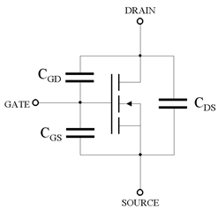
LVCMOS output buffers are, as the name suggests, low-voltage complementary MOSFET outputs. This means that the output stage is derived from a P-channel and N-channel MOSFET in a "totem pole" configuration, see below.

These MOSFETs have some intrinsic parasitic capacitances from gate to drain, gate to source, and source to drain, which vary as a function of applied VGS and VDS voltages. But these capacitances can easily be in the picofarad range in terms of order of magnitude.

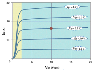
Additionally, each MOSFET has some maximum short-circuit current it can supply based on the gate-source potential that can be applied internally, where the MOSFET hits the linear region and begins to behave like a linear resistor. This might be a few tens of mA.

In order to make for a convenient and approximately correct example calculation, let's say 5pF is the parasitic capacitance and 50mA is the short-circuit current achievable in the MOSFET linear region - this is reasonably close to the actual values for the LMK04832.
Now, consider a 3.3V sine wave at 1GHz. Taking a basic derivative, we know the maximum slew rate of just this sine wave is 2π*Vpk*F, which at 1GHz works out to about 10V/ns. Incidentally, if we take 5pF and 50mA, and consider that I = C * dV/dT, we find that dV/dT = 50mA / 5pF = 10V/ns. Since our output current is limited by the drain-source voltage during the short circuit condition, our output slew rate can never be faster than what is required for a 3.3V 1GHz sine wave.
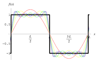
Finally, recall that to get a sharp square wave, we require summing the Fourier series of the fundamental and several of its odd harmonics.

At 1GHz, we are able to get a reasonable slew rate on the fundamental, but the harmonics at 3GHz, 5GHz, 7GHz, etc. all require 3x, 5x, 7x the slew rate for a comparable amplitude sine wave. We cannot supply enough current to achieve comparable amplitude in the higher order harmonics, and so the waveform appears attenuated because the higher-order harmonics that give it a characteristic square shape are attenuated. Edited: I remember there is a factor of 1/n in the Fourier series summation, so actually the slew rate requirements remain equivalent: the amplitude of the 3rd order harmonic at 3GHz is 1/3 of the fundamental, so the slew rate should be sufficient for a decent square wave up to the limits of attenuation. However, the impedance of the parasitic capacitance drops dramatically at higher frequency, and the short circuit MOSFET into a parasitic capacitance looks like a low-pass filter; so the amplitude of the higher-order harmonics is attenuated by 20log(1/n) vs 1/n required for each harmonic of the square wave. And above 1GHz, we would still expect slew rate limitations to impact amplitude.
This is one of the reasons why the datasheet lists the maximum output frequency of LVCMOS as no less than 250MHz - while we can reasonably expect a decently square square wave at 250MHz, above this frequency we would expect a gradual transition to increasingly attenuated sine wave.
There are other reasons, particularly reflections - CMOS output stages have variable impedance as a function of the VDS voltage across the active stage (especially during the transition from linear to saturation regions), which makes higher frequency CMOS signals difficult to terminate at the receiver without a significant reflection component; in continuous operation this creates a standing wave that tends to disrupt the normally monotonic CMOS edges. Careful design with low-capacitance MOSFETs and some resistive damping to attenuate the reflections can sometimes allow for higher frequency CMOS signaling, but generally only at very low voltages where the MOSFET capacitances can be smaller, or within silicon ASICs where the distances between source and load (and therefore the reflections) are negligible and the capacitance is extremely low relative to the actual loading.
In other words, using LVCMOS output format on LMK04832 above 250MHz is not recommended.

Other output formats on LMK04832 use bipolar transistors instead of MOSFETs, and the bipolar transistors have extremely low parasitic capacitance in their active usage mode. Output formats like LVPECL and CML tend to attenuate much less at higher frequency thanks to this lower capacitance, even if the total current load is lower, because C scales much, much lower than I in the slew rate equation (low hundreds of femtofarads is >10x capacitance reduction, vs maybe a 2x or 3x reduction in drive current).
Regards,
Derek Payne