This thread has been locked.

If you have a related question, please click the "Ask a related question" button in the top right corner. The newly created question will be automatically linked to this question.

CDCE6214: y0 always no output

Part Number: CDCE6214

hello,

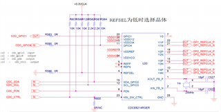
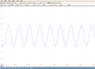
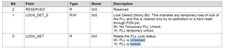
    My schematic is  designed to use a 25MHz crystal as ref clk, after configuration, we can view 25MHz  wavefrom from the crystal pins. but the pll can't lock, so I config Y0 as output and source from refclk. but there is no any signal on CDCE6214 pin7. We also tried to config Y1 source from refclk and still get nothing. so how to debug the hardware? is the amplitude of crystal too small? the oscilloscope shows that the peak-peak voltage is about 1.5V,I thing the amplitude is enough, but why I still can not get the refclk?


  • when select ref_clk, the output of Y0 and Y1 is correct.

    but the pll still  unlocked, the reg7 is  0x40c, 

  • Hi Weihua,

    I did not see any obvious problems on the schematic. 1.5 V differential voltage swing on the crystal should be fine if you are powering the device on 3.3 V or 2.5 V, but it is too high for 1.8 V.

    Can you attach the TICS Pro configuration file (.tcs) that you used to program the device? I would like to review the registers.

    Thanks,

    Evan Su

  • cdce6214.tcs

    the PLL can't be locked 

  • Hi Weihua,

    The input and PLL configuration looks OK. The only unusual detail I noticed is that in User Controls --> Pin Configuration, I see that GPIO1 and GPIO4 are configured as outputs, but your schematic configures one of them as input and the other as output (text says GPIO1 input and GPIO4 output but arrows seem to be the opposite). Not sure if it is related to the PLL issue but I think it is worth checking and correcting if necessary.

    To make sure I am understanding your situation correctly: in your original post you said that when you tried to bypass the crystal into Y0 and Y1, it did not work. In your next post you said that "when select ref_clk, the output of Y0 and Y1 is correct." Does this mean that you can now correctly bypass the crystal and read the output on Y0? Did you change anything to get it to work?

    When the device is active, try recalibrating the PLL (button on top of the "PLL" page) and let us know if the PLL can lock or not afterwards.

    Best,

    Evan Su

  • I have solved this problem, there is a problem with the crystal used earlier, and changing the crystal solves the problem