This thread has been locked.

If you have a related question, please click the "Ask a related question" button in the top right corner. The newly created question will be automatically linked to this question.

CDCLVP111-SP: Yet another question about LVCMOS inputs

Part Number: CDCLVP111-SP
Other Parts Discussed in Thread: CDCLVP111

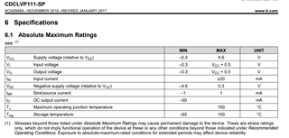
The answers to previous questions about single-ended inputs are inadequate. Is it really true that the max VID for a single leg is 1.3V, such that the part will be damaged by a 3.3V single-ended input connected as shown in Fig. 8? Or is this just a characterization limit, because the part has not been tested with single-ended inputs, and the design would be tolerant to greater swings?

If there really is a risk of damage, the datasheet figure 8 (shown below) is highly misleading. It would only work for a 1.2V LVCMOS output, which is rarely seen in oscillators. But I question whether 1.3V is really the threshold where the part will start to have problems.

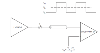
Another problem: in the datasheet, VCM min for CLKn is 1V. In another question/answer, it is stated that this must be satisfied for single-ended input. This appears to completely contradict the picture above, if a voltage division is required. To state the obvious, an LVCMOS signal divided down to 1.3V will have a VCM of 0.65V, which is less than 1V. Reconciling this would require the addition of AC coupling + DC biasing. Please explain these inconsistencies.

  • Hi Azad, 

    The device shouldn't be damaged if VID exceeds 1.3V since that's still well within the absolute maximum ratings for the input pins. 

    From what I can tell by looking through the original validation data, the VID and VCM limits were set for characterization purposes rather than checking functionality. The device will most likely have better performance with LVPECL inputs compared to LVCMOS, so the characterization effort was most likely performed with that in mind. The VID characteristics in Table 6.6 only apply to LVPECL standards/characterization so they can be disregarded for LVCMOS inputs. I would recommend using 2.5V or 3.3V LVCMOS inputs if possible to ensure that VTH > 1V since I can't find information about operating the device with a lower common mode voltage. Note that the original CDCLVP111 was released around 15 years ago and it's difficult to find some information which is why you might see some contradicting information or confusion on different E2E threads. Let me know if this answers your questions. 

    Regards, 

    Connor 

  • Thanks Connor, that is the reasonable answer I was hoping to get. I appreciate the clarification! Such is the struggle of designing with space grade parts :)