- Ask a related questionWhat is a related question?A related question is a question created from another question. When the related question is created, it will be automatically linked to the original question.
This thread has been locked.
If you have a related question, please click the "Ask a related question" button in the top right corner. The newly created question will be automatically linked to this question.
Hi Team,
We are using LMK04832NKDT in one of our projects. Please suggest if we can proceed with the below termination approach & values for the LVDS clock outputs.
 (Split termination of 100E is used here at the destination side).
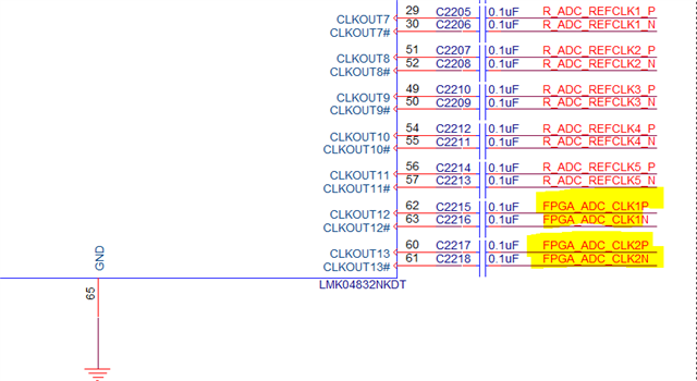
While referring to EVB we found that the capacitors are placed after the termination resistors.
Please suggest if we can place the AC coupling capacitors near the IC itself & the termination (split or single 100E) near the destination.
Or should follow the EVB approach first termination followed by AC coupling capacitor (both at the destination side)?
Please also note that for us the source (LMK) & the destination ICs(FPGA) are placed on separate cards.
Hi Arjeet,
Please refer to the following: https://e2e.ti.com/support/clock-timing-group/clock-and-timing/f/clock-timing-forum/1110184/lmk04832-source-series-termination
Regards,
Vicente
Hi Arjeet,
If you're implementing the above termination as a precaution for HF VCM noise making it's way to the Rx and affecting the biasing point voltage - then your scheme is perfectly fine
Regards,
Vicente
Hi Vicente, I couldn't find any specification regarding internal termination to the output clocks for LMK4832. Can you please help me locate it?
Hi Vicente, I agree with your suggestion. Instead of split termination, can I use a single 100E at the destination?
Would you no longer want to use the cap to filter the HF VCM noise?
But if you don't that it also fine for LVDS Rx.
Regards,
Vicente
I will check for this, if possible I will use it.
Also, I can have the cap first followed by the resistors rite? What if resistors come first then the cap? Will that make any change?
and can you suggest this?
I couldn't find any specification regarding internal termination to the output clocks for LMK4832. Can you please help me locate it?
Arijeet,
Split 50Ω to AC-cap to GND or 100Ω differential is acceptable termination in either case - you might want to confirm there's no internal termination on the destination first though. The split 50Ω and AC-cap to GND approach is sometimes favored when the signal must travel over cabling, backplanes, or longer distances in general, since this helps to filter high-frequency common mode noise.
Cap followed by resistors or resistors followed by capacitors is acceptable to LMK04832. If you place caps first, and you need AC-coupling on the LMK04832 assembly, place the caps close to the LMK04832 to minimize reflections from the impedance discontinuity they'll present. You could also place the AC-coupling caps next to the termination resistor on the other assembly if their assembly location isn't critical. Whatever else you do, aim to keep the 100Ω differential (or split 50Ω) termination close to the receiving device, so that most of the signal power is absorbed right at the receiver with as little stub as possible from termination to receiver.
I'll note that the destination device may have some preference for how its termination network needs to look, which can likely be found in its datasheet or with the device's support team. This is probably the governing factor in whether resistors or capacitors need to come first. It's common for clock receivers to weakly bias the receiving pins with a high-impedance source e.g. some Vbias through 50kΩ, to help ensure operation of the receiver; this may also include slight hysteresis on the receiver pins. The bias and any hysteresis could be impacted by placing resistors after caps. Check with the receiving device's datasheet to confirm termination requirements.
I don't think we list internal termination to the LMK04832 output clocks anywhere; LVDS and HSDS should be close to 50Ω source impedance, but the other formats like LVPECL, CML, and LVCMOS would be low impedance drivers. It doesn't change that our recommendations for LVDS/HSDS termination are 100Ω differential or equivalent.