This thread has been locked.

If you have a related question, please click the "Ask a related question" button in the top right corner. The newly created question will be automatically linked to this question.

LMK1D2102: Clock Recovery over cable

Part Number: LMK1D2102
Other Parts Discussed in Thread: DS25BR150,

Hi,

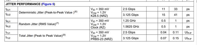
I have a number of very low jitter clocks coming offboard. I am looking for a buffer to restore the clocks in the 100MHz - 1GHz range with the lowest possible jitter.

Is LMK1D2102 suitable for this? Initially I was planning to use DS25BR150 but I see this part has higher jitter?

  • Hello RevKy,

    Yes, the LMK1D2102 should be suitable for getting a frequency and buffering it out to several other parts on your system. However, if it loses it's clock input, the output will no longer be seen until it's obtained again.

    If you'd like to maintain the output clock even when the input is lost, then you need a part that has holdover. You can look at our jitter cleaners and network synchronizers for this functionality. Let me know if you need anything else.

    Good luck,

    Andrea

  • I  am not looking for a holdover. I just want the lowest jitter buffer that takes a degraded clock/data signal  which is transmitted over a cable and restores its eye diagram. I don't understand whether this part does this or not?

  • Hello RevKy,

    Are you cleaning both the data and the clock? My team focuses on clocks, and if you want to clean the clock, then you need a jitter cleaner (linked in previous reply). Please tell me:

    • Output frequencies required and how many?
    • Output type (all LVDS)
    • Output jitter required

    If you also want to clean your data; then, I would recommend creating another E2E thread with DS25BR150 as the part number and the team that supports that part can better support you for that part of your system.

    Best,

    Andrea

  • This is to clean up to 8 channel clock signals coming into the board.

    I have a PLL generating 50MHz, 100MHz, 250MHz, 1GHz.This PLL is on a separate board and the output is LVDS through coax cables hence I expect the eye diagram to be degraded. The cables are approx. 0.5m long. Everything is LVDS input and LVDS output.

    The clocks are all 1:1 going to FPGA. Ideally additive jitter would be below 20ps.

  • Hi RevKy,

    Thank you for this, it seems your sole goal is to obtain a clean eye diagram and not necessarily the clock signal directly. I will put you in contact with the DS25BR150 to better support you.

    Best,

    Andrea

  • RevKy

    Below is the DS25BB150 jitter performance, would this meet your requirement?

    Thanks

    David