This thread has been locked.

If you have a related question, please click the "Ask a related question" button in the top right corner. The newly created question will be automatically linked to this question.

LMK04832-SP: Dual loop performance versus Single loop performance

Part Number: LMK04832-SP

Hello, how are you?


I want to ask you a question. We are working on a design of LMK04832-SP in dual loop mode.We made some tests about that mode and we noticed the PLL2 single loop mode has a better performance than dual loop mode. We are working with PLLatinum, we made all our test in PLLatinum, dual mode and single mode, and we can simulate the PLL2 single loop performance from the datasheet with PLLatinum. See the figures below.

-------------------------------------------------------------------------------------------------------------------------
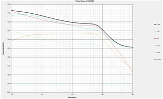
Simulate datasheet performance at 3200Mhz pll2 single mode

-------------------------------------------------------------------------------------------------------------------

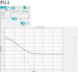
Dual modo perfomance at 1600Mhz

In my Dual mode case, we have a XO of 100Mhz in the input of PLL1, the input of PLL2 is the output of PLL1.

-------------------------------------------------------------------------------------------------------------------

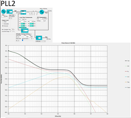
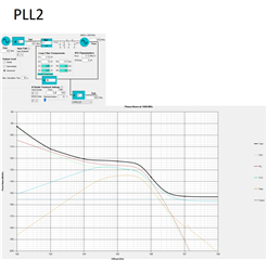
PLL2 Single modo perfomance at 1600Mhz

In my PLL2 single mode case I have a XO of 100Mhz in the input of PLL2.

-------------------------------------------------------------------------------------------------------------------

We've read in the datasheet that the dual loop PLL architecture should provide the lowest jitter performance, but based on our simulations we are obtaining the opposite results.

Do you know why is that? We want to understand why the Single mode performance is better than dual mode.

Best.
Facundo Cosentino

  • There's two things going on here:

    1) PLLatinum Sim measurements were taken from the OSCout port, since this is typically where the VCXO in the PLL1 loop would be extracted to other devices. However, the OSCout buffer noise floor is actually not that great; you can see that the VCXO noise is significantly lower at the floor than the OSCout noise floor as presented in the PLL1 simulation. This means that when you extract the output results of PLL1 and provide it as OSC source to PLL2, you see an elevated noise floor contributing to the PLL/VCO noise total. In advanced simulation mode, you can actually disable the output buffer contribution to the overall noise (or alternately, adjust it to about -167dBc/Hz for the 100MHz case, ±3dB/octave relative to VCXO frequency) and you would get a more accurate representation of the noise floor seen at the OSCin port and the PLL2 phase detector reference port. This explains a lot of the problem you're seeing, but probably not all of it.

    2) If you have a super-clean 100MHz OCXO or TCXO reference, and you try to lock it to a 100MHz VCXO PLL first with the intent of "jitter-cleaning" the OCXO... it's probably not going to improve your jitter, because the OCXO started cleaner than the VCXO could ever achieve.

    The thing TI calls "dual-loop/jitter cleaner" should really be described as a cascaded configuration, which can have jitter cleaning or frequency multiplying effects depending on the input reference characteristics relative to the required outputs. In general, cascading PLLs will necessarily add the noise of two PLLs and two VCOs to your reference. In certain limited circumstances, however, the PLL noise above the loop bandwidth is an improvement over the reference noise below the loop bandwidth. For instance, recovered clocks, or clocks that have excellent close-in offset noise but a terrible output buffer for distribution, might be improved by substituting the high-noise portion of the farther-out offsets with a low loop-bandwidth VCXO. Alternately, you may have an extremely clean 10MHz reference, but require a 2457.6MHz output clock; in this case PLL1 could be used as a low-bandwidth PLL with a low phase detector frequency that stays locked to the 10MHz reference, but which substitutes the large input reference multiplication that would otherwise take place in PLL2 with a higher-frequency 122.88MHz or 245.76MHz VCXO. That way PLL2 phase detector frequency can be maximized and PLL2 loop bandwidth can be greatly increased, which generally pushes down the PLL2 noise contribution; and there's no substantial reference noise multiplication from PLL1, since the loop bandwidth is low enough that nearly all contributing noise is VCXO noise. The key takeaway is that, even though the cascaded architecture is necessarily going to add noise over the single-loop architecture, in certain cases due to suboptimal reference frequency or noise characteristics, the added noise of a cascaded architecture may be less than the reference noise of the single-loop architecture.

    If your reference is clean and close to the maximum acceptable phase detector frequency of PLL2, there's typically no benefit from using the cascaded architecture.