This thread has been locked.

If you have a related question, please click the "Ask a related question" button in the top right corner. The newly created question will be automatically linked to this question.

CDCE813-Q1:Recommended jitter specification for clock input

Guru 19565 points
Part Number: CDCE813-Q1
Other Parts Discussed in Thread: LMK5B12204, CDCE913

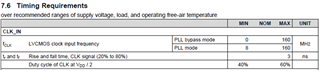
Datasheet P8 is described recommended specification for timing requirements, but jitter specification is not described.

Is there required input spec for jitter?

Best regards,

Satoshi

  • Satoshi,

    In general, for better performance from the PLL, a lower-jitter reference clock is ideal. The higher the phase noise (and in turn, RMS jitter) of the input clock, the more reference noise is able to pass through the PLL to the output clocks.

    Thanks,

    Kadeem

  • Hello Kadeem,

    Is there simulator tool to see output clock characteristics of CDCE813, like TICS pro?

    This time our working condition is that input clock 24.576MHz with 4ns jitter from digital PLL output then we expect jitter reducing function of CDCE813 to get clean 24.576MHz output. What is the best simulation result of CDCE813 output clock jitter?

    We have ran Webench at this condition, the result is attached. LMK5B12204 is recommendation of the lowest cost solution and get 125fsrms output jitter. But it is still little bit expensive and too good performance.


    Regards,

    Mochizuki


    cta-export_2023-11-6_23;42;14.pdf

  • Mochi,

    The CDCE913 lists a jitter specification of 50 cycle-to-cycle, using this may be the best bet.

    There is also an evaluation module available for order, which can be used to determine the jitter performance. There is not a simulator available for this part.

    Thanks,

    Kadeem

  • Hi Kadeem,

    Here is additional question from the customer.

    In Jitter cleaner use case, Vcnt Pin4: "VCXO control voltage" is recommended as leave open or pull up when not used.

    Is that meaning when input external master clock, there is no side-effect even if external noise voltage is injected to Vcnt pin?

    Basically Vcnt pin voltage connect to variable capacitor, there isn't any other connection to PLL function. Is that correct understanding?

    Regards,

    Mochizuki

  • Mochi,

    This is correct. The VCXO control voltage pin VCNT has no effect unless the VCXO input option is specifically chosen.

    Thanks,

    Kadeem

  • Hi Kadeem,

    Thank you for your prompt reply.

    Now our customer's question is close, I appreciate for your help.

    Regards,

    Mochizuki