This thread has been locked.

If you have a related question, please click the "Ask a related question" button in the top right corner. The newly created question will be automatically linked to this question.

CDCE913: Unable to meet the requirements of plus or minus 150PPM.

Part Number: CDCE913
Other Parts Discussed in Thread: CDCE6214

Dear Expert

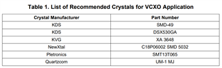
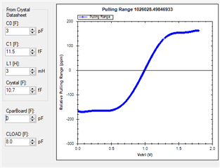
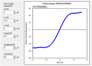
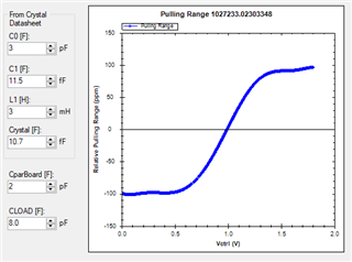
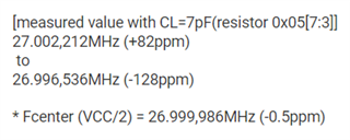
Regarding the application issue of CDCE913 VCXO, based on the previous factory response, we have further debugged it, but it is still unable to meet the requirements of plus or minus 150PPM. Now that the recommended crystal oscillator GSX530GA in the SCAA085 document has been replaced, it still cannot meet the requirements. The pulling range test result is+29PPM~+216PPM. Why is the pulling range all positive? And the maximum and minimum range cannot reach 300PPM. Please help to continue analyzing the problem. Thank you!

CDCE913_VCXO_Voltage Frequency waveform.xlsx

  • Gabriel,

    I cannot find a GSX530GA XTAL - the below list of XTALs from the SCAA085 document are known to be suitable for VCXO pulling applications:

    The minimum pulling range of +/- 120 ppm is strictly for the XTALs listed in this application note.

    The issue with positive-only pulling range may be due to procedure. Please ensure that the below procedure is followed for entering VCXO mode:

    Are the XTALs placed as close the the CDCE913 as possible? Board parasitics will affect the overall pulling range.
    Thanks,
    Kadeem

  • Dear Kadeem

    We didn't use the wrong model, it's DSX530GA .


    We have conducted further debugging on the issue with the procedure. By modifying the internal load capacitor of CDCE913, we can achieve a pulling range adjustment of positive and negative 85PPM, but the range still cannot reach positive and negative 120PPM. According to the original factory's response:

    1. Regarding the question of whether XTAL should be placed as close as possible to CDCE913, these two devices on our board are very close.

    2. The parasitic capacitance at the board level will affect the pulling range, and we are currently unable to determine whether there is an impact of parasitic capacitance at the board level. thanks !

    Below is test date .

    CDCE913_ VCXO_ Voltage frequency curve_ New Debugging (1). xlsx.xlsx

  • Gabriel,

    From the Excel document - external load capacitors are not needed in VCXO mode as the CDCE913 uses the internal load capacitors.

    There can be added board capacitance if there are traces present above/below the XTAL routing. The below excerpt from SCAA085A details best routing practices for minimizing the board capacitance for future designs:

    Note the difference in the Pulling Range plot estimate with added board capacitance:

    I see in another thread that the recommended load capacitance for the device from the manufacturer is 8 pF: https://e2e.ti.com/support/clock-timing-group/clock-and-timing/f/clock-timing-forum/561813/cdce913-cdce913-vcxo-pulling-range/2094912?tisearch=e2e-sitesearch&keymatch=DSX530GA#2094912

    With the same XTAL, they see these results:

    In your measurements ,the largest variation in pulling range is with the 8-pF capacitors. What can be tested is using external C740 and C743 as low values (as an example, 1-pF) and setting the on-chip load capacitance to 7-pF, then adjusting the VCXO voltage and measuring the ppm variation.

    For I2C or pin-based ppm variation with a different part, the CDCE6214 has a digitally-controlled oscillator mode that functions as an easier-to-use version of the VCXO pulling found in the CDCE913.

    Thanks,
    Kadeem