This thread has been locked.

If you have a related question, please click the "Ask a related question" button in the top right corner. The newly created question will be automatically linked to this question.

LMK04832-SP: Powered Off Max Input Voltage

Part Number: LMK04832-SP

Hello,

What is the max input voltage to the LMK04832-SP when it is not powered? Is there also a frequency dependency when powered off?

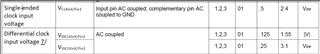
There is a note in the datasheet that specifies the unpowered state of the device:

"(2) When the device is in an unpowered state, the clock input pins (CLKinX/FinX and OSCin) can accept AC-coupled signals up to
±400mV. The absolute limit for an unpowered device input while AC-coupled is determined by the ±5mA (RMS) current limit for the
pins. The ±5mA (RMS) current limit for AC-coupled clock inputs is satisfied across operating junction temperature by a ±400mV
signal coupled through 0.01μF capacitance across allowed operating frequencies. Larger"

Though it also states the max input voltage is VDD+0.3V so if VDD = 0V, then Max input voltage is 0.3V

For my application, the LMK will receive a sine signal on Fin0. Fin0* is ac-coupled to ground. 

Thanks!

  • This is tricky to pin down exactly.

    We did some analysis and determined that above ±5mA rms, at the upper end of the ambient temperature range, it was possible to see electromigration issues long-term in the metal layers around the input ESD structure. Of course, when you're AC-coupled into a diode clamp from a nominal 50Ω source driving at tens or hundreds of MHz, it can be very challenging to determine the exact RMS input current! Moreover, the VDD input clamp will also backdrive the supply voltage for the device; in practice, this means the load impedance near the top of the rising edge of each input cycle will vary dramatically as more junctions internally climb up their exponential I-V curves. This also implies that some current can exit the VDD pin and back-drive any other impedances on that VDD line. On top of that, larger input coupling capacitors and higher frequencies will result in more charge transferred per cycle of the input waveform.

    Given the dependencies on frequency, voltage, amplitude, and input coupling capacitance, as well as the complex nature of the impedance on the other end, it's infeasible for us to define an input limitation as a function of purely voltage - in some cases this depends on external circuitry outside of our control. So we offered an RMS current limit for the pins, because this is at least plausible to measure (insert a small resistance in series with the driver and measure voltage across the resistance with a differential probe) and has a known correspondence to the power dissipation within the ESD metal routing that results in electromigration issues.

    I'll also point out that if the ambient temperature can be restricted, you can improve the current-handling capacity by around double the RMS rating per 20°C. This is very much an estimate and it starts to fall off at 50°C once the I2R effects in the metal layers start to add up, but it might build confidence if you know the ambient temperature will never exceed certain limits.

    I realize this makes it difficult to anticipate the exact behavior of the LMK04832-SP when unpowered and subjected to an input stimulus, but the architecture of the LMK04832-SP is such that we can't simplify the problem any more than that. We did one simulation by request for the ±400mV input case, with the worst-case assumption that VDD was tied to ground, at 100MHz, with 0.01µF AC-coupling capacitance, and confirmed that this didn't cause any problems across the allowable ambient temperature range. If your use case doesn't resemble this simulation, let me know the expected input amplitude, frequency, and anything else that might be back-driven by the VDD on LMK04832-SP, and I can at least tell you if you're in the ballpark for acceptable unpowered input stimulus.

  • Hi Derek,

    The expected amplitude is ±300mV

    Frequency = 1GHz

    The expected junction temperature = 105°C

    Please let me know if you need anything else.

    Thanks,

    Robert

  • For an amplitude of  ±300mV, at 1GHz and 105°C, there should be no cause for concern.

  • Thank you.

    Just to be make sure this applies to the Fin0 and Fin0* pins?

    Do the CLKinX pins have different limitations? Asking because the specifications for CLKinX and fin0 are separated in the datasheet.

  • Yes, this is applicable for Fin0/Fin0*.

    There is a structural difference (presence of a MOS mode biasing and LOS circuitry on CLKinX, slight biasing adjustments for differential/single-ended input selection on Fin0) but in practice this doesn't end up significantly impacting where the acceptable RMS current threshold is for the input.

    The major differences in the datasheet between CLKinX/OSCin and Fin0 are frequency limitations, which are more a function of the circuitry that follows each input - while Fin0 goes directly to a CML clock distribution network, CLKinX and OSCin may go to R-divider or N-divider circuitry which has input limitations, and the LOS circuitry will encounter issues above some frequency limit in some cases. In practice they're nearly the same bipolar input stage in all cases, just with some biasing circuit differences for the different operational modes. This is reflected in the input amplitude ratings - you'll see that Fin0 and CLKin1 used as Fin1 share identical amplitude requirements.

  • Thank you! appreciate the detailed response.

  • Hi Derek,

    Follow up:

    Fin1 includes specs for both SE and DIFF operation (to confuse things more they have 2 ways to measure differential voltage):


     Fin0 is spec’d only for DIFF operation.  We use it in SE operation, based on their definition.


    So my questions are:

    1. Does the Fin0 pin have the same SE input spec as Fin1 pin ? (i.e.  0.5 to 2.4 Vpp operational voltage ….. -2 dBm to 11.6 dBm)
    2. Do we compare the + 300 mV damage threshold (600 mV pp …. -0.46 dBm) to the SE or DIFF number ?
  • Does the Fin0 pin have the same SE input spec as Fin1 pin ? (i.e.  0.5 to 2.4 Vpp operational voltage ….. -2 dBm to 11.6 dBm)

    Yes.

    Do we compare the + 300 mV damage threshold (600 mV pp …. -0.46 dBm) to the SE or DIFF number ?

    Single-ended. It's a per-pin threshold.