This thread has been locked.
If you have a related question, please click the "Ask a related question" button in the top right corner. The newly created question will be automatically linked to this question.
Hello,
As described in a previous post (e2e.ti.com/.../lmk5b33216evm-tics-pro-settings-not-applied-on-lmk5b33216evm) we have a LMK5B33216EVM board and we would like to prototype a wireless synchronization system. We have given up the 1-PPS part described in that post (we are going to implement it on the FPGA in the controlled system) for a multitude of reasons.
However, we are still interested in having a 10 MHz signal externally controlled in both frequency AND phase, with high accuracy and stability.
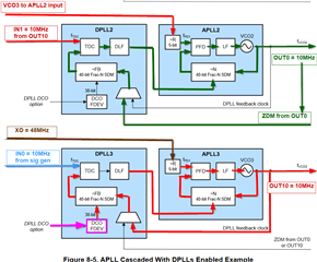
This is the idea that we have in mind --- since, if we understood correctly, activating ZDM prevents us from adjusting the frequency (both because the GCD between the input and output frequency will not be the input frequency anymore, and because the phase lock would prevent the output to change in frequency):
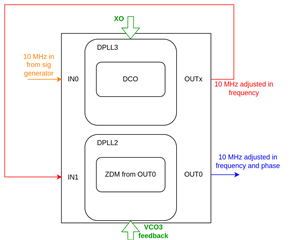
In the diagram OUTx is any output (we have chosen OUT4) and gets fed back to IN1 (avoiding this external loopback would be great, but we have found no way to internally loop back the frequency-adjusted signal).
We have a couple of questions:
1. In the IN1 field of TICS Pro we have set 10 MHz as input frequency but, given that the frequency is altered on the fly by DPLL3, it will not be 10 MHz (or, at least, not the same "10 MHz" that is present on IN0). We assume that the value given here is just to set the different DPLL/APLL parameters and, given that DPLL2 only has to output a signal with the same frequency as the input, it will not complain. Is this correct?
2. We have created the following configuration:
desired_config.tcs
The board, however, does not lock...
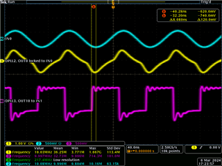
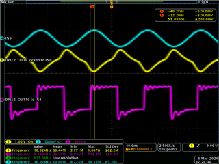
Here is what we can see on the scope (1: 10 MHz input from signal generator, 2: OUT4_P, 3: OUT4_N, M1: math function (green-blue), 4: OUT0):
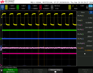
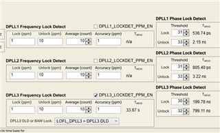
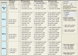
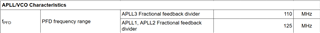
The status gives this (confirming what we observe):
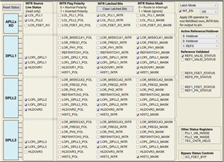
What are we doing incorrectly?
Thanks a lot in advance and best regards,
Rob
Hi Rob,
Let me look into this and get back next week.
Some questions:
Regards,
Jennifer
Hello Jennifer,
Thanks for your quick reply!
1. the RF systems we are controlling has quite accurate oscillators, let's bound their precision to +-0.2 ppm @ 25 MHz, so at most +- 5 Hz (though typically way smaller than that, the highest value I've experimentally observed in more than 1 year was slightly below 2 Hz)
2. actually that was something weird: once I write the registers an output is shown, though it has the wrong frequency. As soon as I hit the software reset, the output disappears, and nothing I can do is able to restore it. Sometimes having the board power cycle + disconnecting the USB and then redoing the programming again, gets back the output, but with the same phenomenon (i.e., when I do the software reset, the output is gone forever). This does not happen if I use a single output, with no loopback, so this is definitely related to a misconfiguration.
3. perfect, thanks for the info!
Looking forward to hearing from you!
Have a nice weekend!
Rob
Thank you for the update. I will review next week as mentioned.
Regards,
Jennifer
Dear Jennifer,
I wonder if you had time to have a look at the issue I encounter, and if further tests are required from my side to give you additional information. I will be at the office tomorrow and so I'll be able to perform them (next week I will be away for mandatory training, so I won't be able to access the board until next Friday).
Thanks a lot and have a nice day!
Best,
Rob
Hello Jennifer,
I've accidentally discovered that the absence of the output is linked with the "Bypass" and the "Doubler" options being checked in the VCO3 feedback for DPLL2 in step 1 --- if I remove both of them, the APLL frequency drops to ~104 MHz, but I see the waveforms as output. However, even though the waveform seems to be very stable on the oscilloscope, it never locks in the status page.
The configuration I've created for this is this one:
(please note that I've changed OUT4 for OUT1 as an intermediate output --- the hw had been changed as you've instructed me in a previous post to have a proper CMOS output on OUT1_P).
Possibly as a consequence of the lack of lock, it seems to be impossible to alter the phase of DPLL2 via ZDM --- the waveform for the final output does not move a bit.
Do you have any idea for the above?
Thanks again for your help and have a nice week-end!
Best,
Rob
Dear Jennifer,
Sorry for being quite spammy today.... but now it works!
The issue with DPLL2 not locking was due to a misplaced cable, wiring it correctly made everything work as expected.
Still, as soon as I set the bypass, the output disappears. If I've understood correctly, having a higher APLL frequency leads to better performance but, apparently, my system is unable to lock even with a divisor set to 10 instead of 12 (in this particular case only the DPLL2 does not lock, while with lower values no DPLL is able to lock). Do you have an explanation for this phenomenon or a recommendation?
Thanks in advance and have a nice week-end!
Best,
Rob
Hi Rob,
My apologies, I meant to reply yesterday and didn't hit send!
Can you please try with this configuration file? This setup is based on your block diagram.
LMK5B33216_XO=48MHz_REF=10MHz_OUTs=10MHz, VOD=800mV, zdm.tcs
However, I do have some additional comments about your block diagram:
Regards,
Jennifer
Dear Jennifer,
No worries, thanks for your reply!
I've quickly tried your design before leaving for the training and it performs similarly to the design I've joined to my latest posts, but it looks like I cannot alter the phase of DPLL2. The diagram in (2), however, does exactly what I do in the above-mentioned design (I use OUT1 instead of OUT10, but the rest is the same), so I'm happy that I didn't stray too much :)
1+4. Yes, this is what we want to achieve. The idea is that IN0->OUT1 uses DCO to adjust the frequency, while IN1->OUT0 adjusts the phase via ZDM. Our goal is to have a 10 MHz signal controllable both in frequency and in phase via I2C (e.g., we would like to be able to just say "ok, increase the frequency of the signal currently output by OUT0 by 1.23456 Hz and the phase by 7.89 ns"), the absolute frequency of the input coming from the signal generator is uninteresting to us --- the 10 MHz output by OUT0 is then fed into an SDR where it gets transformed in a 25 MHz signal, and we want this 25 MHz signal to be "perfectly" synchronized with the 25 MHz used by another SDR device.
Things start to work, now I just wonder why bypassing the R divider & doubler for APLL2 seems to prevent all the PLLs in the board to lock. Do you have an explanation for that, please?
Thanks again for your help and best regards!
Rob
Hi Rob,
When setting the PFD, you want to make sure to stay within the datasheet defined limits.
Additionally, make sure that every time you update the R divider and doubler settings, that you run through the remaining steps in the Start Page again, specifically these buttons:
Can you please confirm if you tried this?
Regards,
Jennifer
Hello Jennifer,
Sure, when I'll be in my office on Friday I'll try them!
Thanks and have a nice day!
Best,
Rob
Dear Jennifer,
Yes, you've nailed the issue, I did not consider the PFD limits
Thanks a lot for your help and have a great week-end!
Best,
Rob