LMK04828: Need support for operating LMK04828BISQ as an LVPECL driver

Part Number: LMK04828

Hello Team,

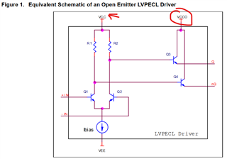
Would like to operate the LMK04828BISQ as an LVPECL driver into a NB7L1008M with as few components in the path as possible. There is a preference to connect them directly as a DC coupled path to minimize "noise". Three paths will be used one at 10 MHz, another at 500 MHz, and the remaining one at 2GHz. Can you assist in describing exactly what is needed to accomplish this?

Regards

Vraj T

  • Hello Vraj,

    Connecting them in DC-couple is more dependent on the input requirements of the NB7L1008M. If the LVPECL outputs of the LMK04828 are within spec for the input requirements for the NB7L1008M, there should be no problems.

    p. 22 of data sheet:

    However, to double check I would contact the manufacturer of NB7L1008M to ensure this is true for their part. Hope this helps.

    Also, do note that we recommend to use AC-coupling to avoid what I explained above, any bias mismatching or overloading on the receiver.

    p. 105 of data sheet:

    Good Luck,

    Andrea

  • Hello Andrea,

    Have you heard back from OnSemi on this?

    Regards

    Vraj T

  • Hello Vraj,

    I cannot speak for OnSemi part, I was speaking from our part having any driver with the characteristics from OnSemi. So no, I have not heard from them on this.

    Best,

    Andrea

  • We have a few more questions from the customer:

    Related, to the TI LMK04828BISQ, can the LVPECL mode be powered at 2.5V rather than the main 3.3V?

    What I need to know is whether that is a safe operating condition and is if there is an application note showing the equivalent output driver circuit.

    I found a model from Renesas that clearly isolates the output voltage to the driver from the internal digital logic rail.

    If the output for the clocks in the LMK04828BISQ is similar I should be able to power the outputs at 2.5v and not have the voltage domain change.

    Please respond

  • Vraj,

    I am taking over this question while Andrea is out of office.  In regards to your original question.  Yes, it it is possible to DC couple a LVPECL into your other device.  The first place to look as Andrea mentioned is the input requirements for your other device.  

    For the NB7L1008M, it looks like the specs we need to meet are the common voltage range, and the voltage high/low.  If your goal is to use as few components as possible it seems like it might be easier to set the LMK04828 in LVDS output mode and then dc couple directly into the NB7L1008M as shown in their datasheet.  

    You will not need to change any Vcc values on the LMK04828.  And if you want a comparable CML clock buffer suggestion.  TI offers the CDCL1810 series of buffers which offers 10 CML outputs with additional divider functionality.  

    Let me know if you need more support.

    Will

  • Hello Willam,

    Thanks for looking into this, the customer wants to confirm more about this product, here are the further comments "

    "Do you have a semi-detailed LVPECL/LVDS clock output equivalent circuit that shows what the driver looks like so I can model it in LTSpice?

     "In more detail, it would show the open collector (open source if only the high side FET is used) along with any protection diode when the LVPECL is enabled.

    It would also show the totem pole FET output structure when the LVDS is enabled.

     What I’d really like is TI’s equivalent circuit for the

    DCLKout0(p/n) and corresponding VCCx_CGy

    SDCLKout1(p/n) and corresponding VCCx_CGy

    SDCLKout3(p/n) and corresponding VCCx_CGy

    SDCLKout9(p/n) and corresponding VCCx_CGy

     Similar to this diagram.


    The data sheet shows there are four separate power pins associated with specific output drivers (VCCx_CGy grouped with DCLKout and SDCLKout pairs. 

    If they are similar to the example above and independent from, the internal logic VCC used upstream of them, then I may be able to match the output driver voltage to the downstream buffers' power rails.

     I know I may be drilling down further than the average engineer but I need to explain it to our customer for SI performance."

    Thanks 

    Vraj Talati

  • Vraj,

    I will ask our design team for this and get back to you.

    Regards,

    Will

  • Vraj,

    I spoke with our design team. Unfortunately, you cannot have a different voltage applied at the output power pins.  The output stage supply can not be separated from its pre-driver stage power supply since they are shorted together on chip.  

    Also, for best way to simulate the output driver would be to use our IBIS model.  We do not usually offer SPICE models for clocking parts.  

    Regards,

    Will