This thread has been locked.

If you have a related question, please click the "Ask a related question" button in the top right corner. The newly created question will be automatically linked to this question.

TLC555-Q1: Will the generated inrush current affect the OUT pin of TLC555QDRQ1?

Part Number: TLC555-Q1
Other Parts Discussed in Thread: TLC555

Tool/software:

Hello,


Currently, in the process of using TLC555QDRQ1, we need to confirm some technical related issues, as described below:

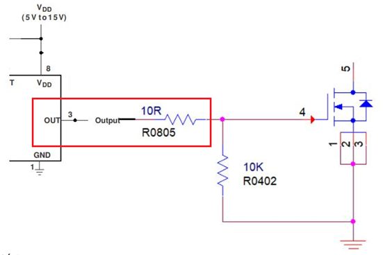
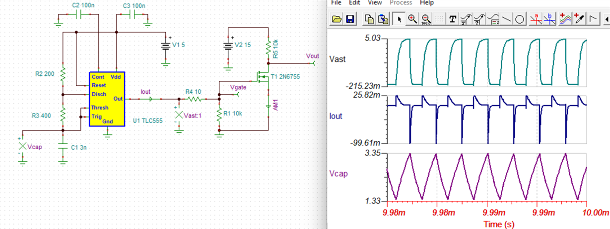
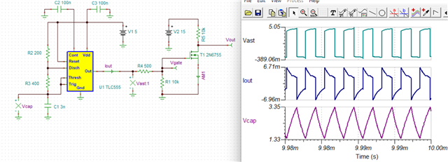
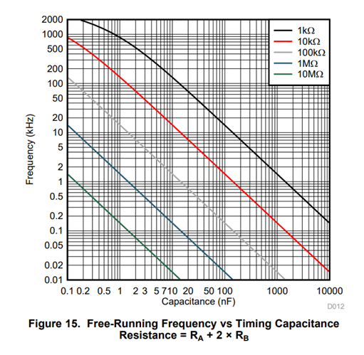
Question 1: We use TLC555-Q1 to drive MOS (MOSFET, N-CH, 2.9A, 100V, DMN10H170SFGQ-7). Connect a 10Ω to MOS at the OUT pin of TLC555QDRQ1, and the frequency is about 500Khz. During the fast switching process of MOS, the TLC555QDRQ1 driving power supply 15V is loaded on 10Ω. Will the generated inrush current affect the OUT pin of TLC555QDRQ1?

Question 2: If the internal resistance of TLC555QDRQ1 is taken into account, will the inrush current affect the OUT pin of 555?

Question 3: If long-term use or aging life is considered, will the inrush current in this scenario affect the OUT pin of TLC555QDRQ1 multiple times?

  • Hi,

    Everyone who can answer these issues?

  • Hi Ethan,

    Thank you for your patience. This is a relatively nuanced question with multiple parts, so I will need some additional time to construct an answer for you. I will get back to you before the end of the business day with an update.

    Best Regards,

    Alex Curtis

  • Hi Ethan, 

    I have simulated a version of the circuit using an available FET in Tina. It does appear that the in rush current does affect the output. For this reason the customer may consider adjusting R4. I do not have a model of their FET to use however the general guidance below may be sufficient. 

    R4 = 10 ohm:

    Using a 10 ohm resistor I am seeing large current spikes on the output. The timer waveform does reach logic levels however you can see that it is not a square wave. 

    R4 = 10k ohm:

    Increasing R4 cleans up the output waveform (more square) and also limits the Iout current to within the 10 mA sourcing current that the TLC555 can supply. The output voltage waveform provides sufficient logic levels as shown below.


    If there is any inductive load the FET is driving you may consider adding TVS diodes on the output of the timer in order to protect the output from going above the supply voltage due to inductive kickback. We have a series on EOS within our TIPL series that discusses component selection. 

    TIPL Series:

    https://www.ti.com/video/series/precision-labs/ti-precision-labs-op-amps.html

    Operating at high frequencies:

    It is very difficult to achieve accurate results above 100kHz and you must use the equations in the PDS that account for propagation delays in order to estimate the timing. These equations are shown on page 17. I have found the propagation delays on the units I measured to be 215ns for both TPHL and TPLH. The values can vary up to 30%. 

    Below you can see that there is significant curvature (non-linear) behavior at frequencies above 100kHz and the timing capacitor needs to be small for high frequencies. For this reason the tolerance of the capacitor must be well controlled and board parasitic capacitance must be accounted for. My recommendation is to use an LCR meter to measure the timing capacitor at the frequency of interest and also measure the board parasitic capacitance with the TLC555 removed from the board. This will give the most accurate result in the equations when plugging in this total capacitance for CT. My recommendation is to use these equations in excel and plugin the real measured values. In addition you should account for the tolerances of components stated from the manufacturer. The timing capacitor is critical and should be film or COG/NPO. The tolerance of the capacitor will be given as 5% in some cases but it is important to measure at the frequency of interest as well to get an accurate value to plug in.  I have attached my example calculator with some values already plugged in for demonstration such as the propagation delays and board parasitic capacitance of my board. See the excel sheet below. Lastly, in the calculator I also calculate the duty cycle at the particular frequencies. You will notice that it is roughly a 60% duty cycle in this case. 

    There are some general best practice guidelines to follow for minimizing parasitic capacitance in the layout of the PCB.

    1. Increasing space between adjacent traces
    2. Cutting out power and ground planes above and below critical traces
    3. Minimizing component to component trace lengths. Shorter traces will have less capacitance due to capacitance per unit length.
    4. Minimizing use of Vias on critical traces.

    TLC555 Equations (1) (3).xlsxTLC555 500 kHz.TSC

    Best Regards, 

    Chris Featherstone

  • Hi Chris,

    Very thanks for your kindly reply. So detailed and so great!!

    The customer wants to know that the output pulse source current of TLC555-Q1 is 133mA, and the output sink current is -443.68mA. Is there any problem with this application for TLC555-Q1 itself?

    Best regards!

    Ethan

  • Hi Ethan, 

    I don't have an answer on pulse current since this device is 41 years old and any data is limited to the product datasheet. 

    The abs max for sourcing and sinking is shown below. Operation outside of these abs max specifications may cause permanent damage.

    Best Regards, 

    Chris Featherstone