This thread has been locked.

If you have a related question, please click the "Ask a related question" button in the top right corner. The newly created question will be automatically linked to this question.

LMK04828BEVM: Using the SYNC input causes all active clock outputs synchronization

Part Number: LMK04828BEVM
Other Parts Discussed in Thread: LMK04828, LMK04826

Tool/software:

hello,

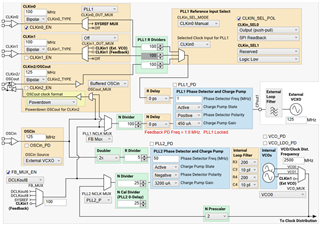
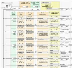
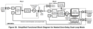
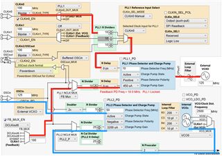
Our current application is to synchronize all the input and output clocks of the LMK04828,  and the phases are aligned after the sync signal is controlled;

Now there are 3 questions : 1. The input and output are not synchronized, and the phase difference is also not fixed (it will change after each power-on restart). 2. After the sync signal is controlled, the waveform can be seen to flicker on the oscilloscope, but there is no change. 3. Is there a timing requirement when configuring registers for SPI?

【Current configuration】

  • Hi Fan, 
    The AE is OoO - 
    Give us until end of week - sorry about delay. 

    Best regards, 

    Vicente 

  • Hi Fan,

    I suspect that you may be using nested zero-delay dual-loop mode, when you should be using cascaded zero-delay dual-loop mode. You can select dual loop 0-delay cascaded mode in the Set Modes menu in TICS Pro. However, I put together a config that may be what you need. I would prefer if you could send over your configuration, so that I can be 100% positive it is what you need, but this should be enough to make sure you have a deterministic relationship between the reference and output phase.

    Thanks,

    Michael

    dual_loop_0_delay_cascaded.tcs

  • Hello Michael,

    Thank you for your reply. The current configuration is configured LMK04828 to Nested Zero-Delay Dual-Loop Mode. All outputs are configured as Device Clock Output (CLKIN0  = 100MHZ; VCXO = 125MHz; CLKOUT = 100MHz) ; I want to use the SYNC input(SYNC pin, without using the sysref function) to trigger the synchronization of all output clocks.

    SystemBoard_HexRegisterValues_PA1.txt
    Fullscreen
    1
    2
    3
    4
    5
    6
    7
    8
    9
    10
    11
    12
    13
    14
    15
    16
    17
    18
    19
    R0 (INIT) 0x000090
    R0 0x000010
    R2 0x000200
    R3 0x000306
    R4 0x0004D0
    R5 0x00055B
    R6 0x000600
    R12 0x000C51
    R13 0x000D04
    R256 0x010019
    R257 0x010155
    R258 0x010255
    R259 0x010300
    R260 0x010400
    R261 0x010500
    R262 0x010670
    R263 0x010711
    R264 0x010819
    R265 0x010955
    XXXXXXXXXXXXXXXXXXXXXXXXXXXXXXXXXXXXXXXXXXXXXXXXXX

    BR//Fan

  • Hi Fan,

    I will get back to you soon.

    Thanks,

    Michael

  • Hi Fan,

    I have reconstructed your setup and tested it in lab. I have had no issues with synchronization, and I think that yours are the result of not synchronizing your dividers. What do you mean when you say you are controlling the SYNC signal? You can synchronize your dividers by pressing the "SYNC Dividers" button in the SYNC/SYSREF tab. Please let me know if you have anymore questions.

    Thanks,

    Michael

  • Hello Michael,

    Can you show your oscilloscope test waveform?

    In my tests, I wanted to use the sync pin inversion to control the synchronization process, and the manual supports connecting external signals via sync pin, or SPI. This test way is my final application.

    There are three problems in my lab bench:

    1. The waveform between the output channels cannot be aligned, and there is a little deviation;

    2. The input(CLKin0) and the output(DCLKoutX) cannot be aligned, that is to say, it is not 0-delay;

    3. After power cycle, these waveforms will be phased shifted.This results in inconsistent results every time.

    The blue is the input(CLKin0), and the red and green ones are the two channels(DCLKoutX) of the outputs:

    BR//Fan

  • Hi Fan,

    Sorry for the delay. I had to perform a rework to board in order to allow for the VCXO to be input as 125 MHz. I will get to you tomorrow.

    Thanks,

    Michael

  • Hi Fan,

    The scope shot that I took can be seen below. The yellow sinusoidal signal is the CLKIN0 input signal and the other two are DCLKoutx outputs (blue is 10, orange is 0, respectively). There will be some skew and delays that are the result of wiring and traces that cannot be removed. 0-delay is actually a bit of a misnomer; 0-delay mode actually means that the delay between the input and feedback output (and any outputs synced to that feedback output, which can be selected in the SYNC/SYSREF page by clicking the appropriate SYNC_DISx boxes) will be deterministic. You need to ensure that you are syncing your dividers upon each power cycle to make sure your outputs are phase-aligned. 

    I have attached my config file (which is for a LMK04826, which is very similar to the LMK04828 but needs to be translated to a config for a 4828) for more clarification. Furthermore, I would like to see your schematic/setup. Are you using an EVM board? If so, have you reworked the board so that your external VCXO is 125 MHz?

    sub_vcxo.tcs

    Thanks,

    Michael

  • Hello Michael,

    There are a few more points that I need to confirm from your:
    1, Is the input signal generated with a signal generator?  or by XO?

    2, the waveform is seems not quite right, the oscilloscope's C3 does not show, the M1(orange ) in the graph should be the result of the math function, right?

    3, the amplitude of the two DCLKoutx in the waveform is not consistent, the relative difference is nearly 1.5ns. The difference in the output result between the two channels is too big.

    4, the EVM can be through the TICS pro to control the sync function, but for the formal application, how do we control it, according to the TICS pro export file can be executed or need to add the sync step in the end?

    5,For the power cycle, we fixed the SPI control program into the FPGA to control the LMK04828, and then the whole system together to carry out the power cycle operation. The phase change between the two output channels occurs at the fifteenth.You can help with the experiments on your end, too.

    We haven't applied for our EVM yet, some of our current experiments are referencing the EVM to make our own boards, I'll send it to you privately and you help to review the schematic, thanks a lot!

    BR//Fan

  • Hi Fan,

    1. The input signal is generated by an SMA100 signal generator.

    2. M1 is a math signal - it is C3 - C4, where C3 is the non-inverted output from DCLKout0 and C4 is the inverted output from DCLKout0. 

    3. The difference in amplitude is due to the way I fed the signals into the oscilloscope. C2 was measured by taking the two outputs from DCLKout10 and sending them through a balun, whereas M1 was measured by inputting each differential signal to the oscilloscope and relying on the math function to resolve the signal. I will see if I can find an additional balun, so that the amplitudes will be the same, and I can send an additional scope shot. The skew is also a bit larger than it should be, I can resolve that too.

    4. The SYNC function can be controlled through various methods (see section 9.7.3.10 in the LMK04828 datasheet), but the easiest method would be to set SYNC_MODE to 1 and input a rising edge to the SYNC pin. That rising edge serves as the "SYNC event" which will synchronize all of the selected output dividers (selected by the SYNC_DISx bit, where x corresponds to the CLKoutx channel, which will be synchronized upon the SYNC event so long as SYNC_DISx is set to 1).

    5. I am a bit confused by what you mean here. The phase change between the two output channels occurs at the fifteenth occurrence of what? Have you tried synching the dividers when that happens?

    Also, you are more than welcome to send any questions or schematics to my email, m-srinivasan@ti.com :)

    Thanks,

    Michael

  • Hello Michael,

    Thank you for getting back to me. I'm going to continue tracking our issue with email.

    BR//Fan