CDCM6208: Reference clock not detected

Part Number: CDCM6208

Tool/software:

Hi. I am trying to get a CDCM6208 working on a newly spun board. I used the CDCM6208 application and evaluation board to generate and verify settings, and it all seems to work without issue there.

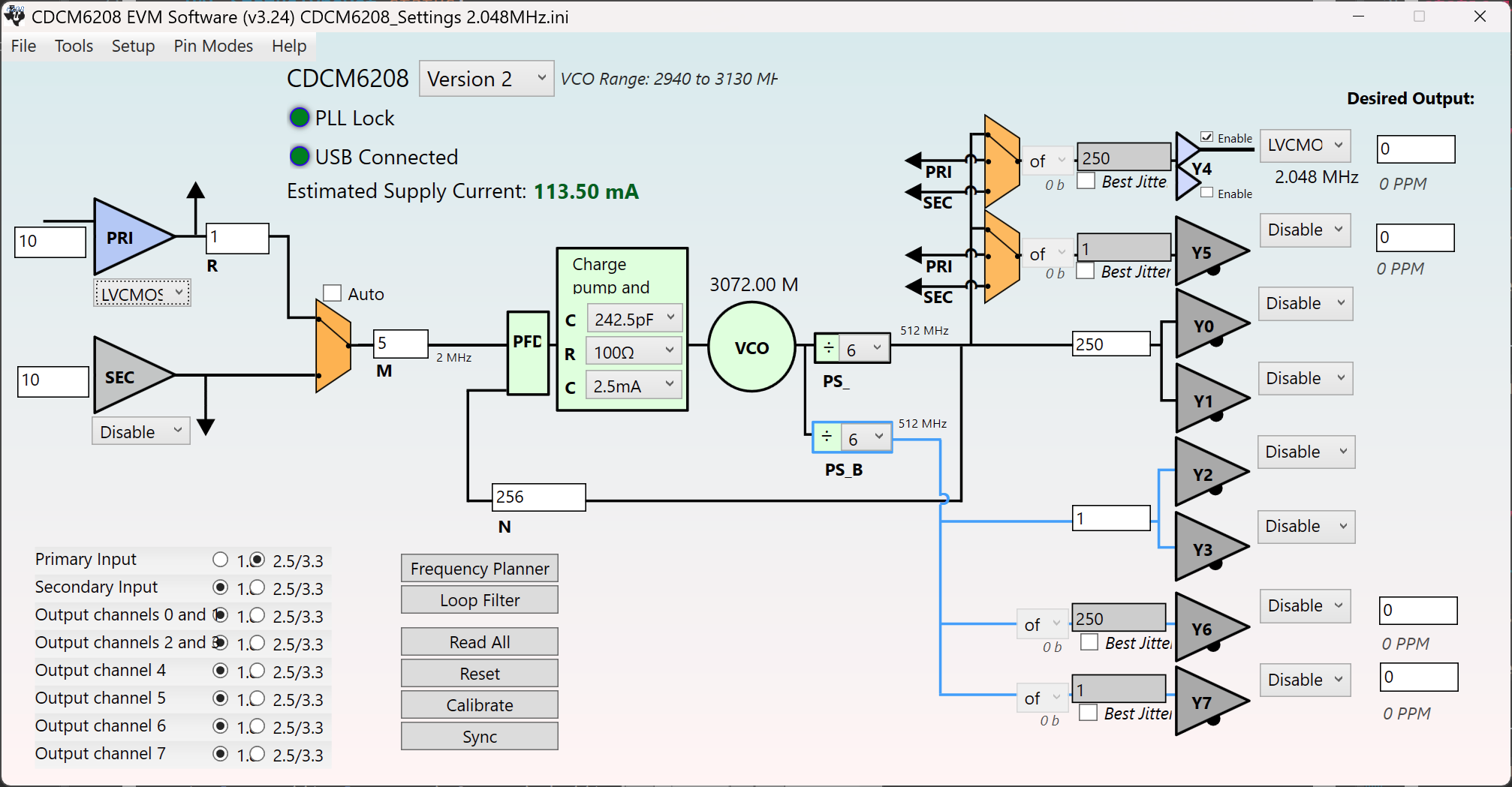
On my own board, the loss of reference bit is always set in the status register (0x0006). I programmed the registers in order using the values from this application, and tried toggling the reset but in register 4.

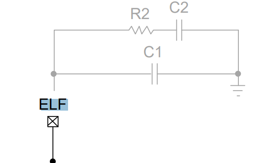
My schematic looks like this:

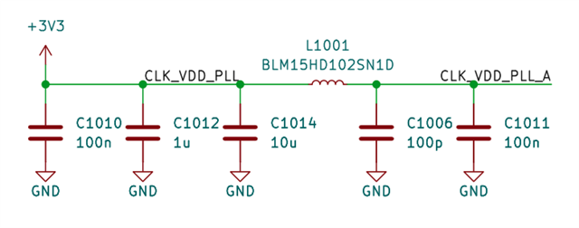
I have verified that REF_SEL is high, and that a 10MHz reference signal is on pin 8. The reference looks good, a solid square wave, 0 to 3.3V. Powers supplies look good as well.

I tried various settings for the MUX, but none seem to have helped.

Any assistance would be greatly appreciated.

  • Paul,

    I will test this config on the bench tomorrow. But from looking at the schematic, do the I2C lines have pullups to 3.3V? These are necessary for proper communication with the device. 

    Is there a reason a single clock output is being used to drive two separate loads?

    And just to confirm, both the EVM you used to test and the custom board are using a V2 part, correct?

    Best,

    Cris

  • Hi Cris.

    Thanks for taking a look. Yes, the I2C lines have pull ups and the bus is working correctly. I can read the chip ID and status information, and program the other registers.

    The single output is used with buffers to ensure that both have the same phase. I could revise it but I don't think that is the cause of the reference not being detected.

    Yes they are both the V2 part. The ID register confirms that this is a V2.

    Thanks.

  • Paul,

    Thank you for your response, I just wanted to exhaust all possible options.

    From what I see on the bench, sometimes when the PLL is unlocked the part will also show the LOS bit as 1, even if the reference input is still there. 

    I used the CDCM6208 application and evaluation board to generate and verify settings, and it all seems to work without issue there.

    Can you export the exact register file from the GUI when you had the EVM working? I will continue to work on the bench on my side but the register dump would be very helpful.

    Additionally, does buffering PRIREF to the output show the signal? Or does the output remain muted?

    Best,

    Cris

  • Hi Cris.

    Thanks for your response. Here is the .ini configuration file content:

    Fullscreen
    1
    2
    3
    4
    5
    6
    7
    8
    9
    10
    11
    12
    13
    14
    15
    16
    17
    18
    19
    20
    21
    Register 0: 01B9
    Register 1: 0010
    Register 2: 00FF
    Register 3: 08FA
    Register 4: 208D
    Register 5: 0000
    Register 6: 00F9
    Register 7: 0000
    Register 8: 0000
    Register 9: 0052
    Register 10: 0F90
    Register 11: 0000
    Register 12: 0000
    Register 13: 0000
    Register 14: 0000
    Register 15: 0050
    Register 16: 0F90
    Register 17: 0000
    Register 18: 0000
    Register 19: 0000
    Register 20: 0000
    XXXXXXXXXXXXXXXXXXXXXXXXXXXXXXXXXXXXXXXXXXXXXXXXXX

    I will try buffering the reference and get back to you.

  • Okay, sending the reference to the output works. So it seems that the reference is actually working. However, the LOS bit remains at 1. I also don't get any output from the PLL if I switch back to that.

  • Paul,

    Thank you for the I2C dump.

    If you write the following config to the device on your board, do you see the proper output on Y4?

    Can you also provide the portion of the schematic that shows the REFCLK?

    3482.HexRegisterValues.txt
    Fullscreen
    1
    2
    3
    4
    5
    6
    7
    8
    9
    10
    11
    12
    13
    14
    15
    16
    17
    18
    19
    R0 0x000001B9
    R1 0x00010010
    R2 0x000200FF
    R3 0x000308FA
    R4 0x0004208D
    R5 0x00050000
    R6 0x000600F9
    R7 0x00070000
    R8 0x00080000
    R9 0x00090052
    R10 0x000A0F90
    R11 0x000B0000
    R12 0x000C0000
    R13 0x000D0000
    R14 0x000E0000
    R15 0x000F0050
    R16 0x00100F90
    R17 0x00110000
    R18 0x00120000
    XXXXXXXXXXXXXXXXXXXXXXXXXXXXXXXXXXXXXXXXXXXXXXXXXX

    Best,

    Cris

  • Paul,

    I have done some additional bench testing. Based on my findings, the config I sent previously should provide the correct output, but in future applications we recommend pulling the unused PRIREF channel to GND in order to ensure best device performance and functionality.

    Best,

    Cris

  • Hi Cris.

    Thanks for the settings. I have tried them but am still not getting any output. I will see if I can bodge PRIREF to GND.

  • Hi Chris.

    I have connected PRIREF_N to GND, but it didn't help. I have also read back all the registers and confirmed that your values were properly programmed into them.

    Here is the part of the schematic you asked for:

    The CSAC is an atomic clock providing a very stable, very accurate 10MHz. It is then buffered and REF_CLK2 is routed to the PRIREF_P input of the CDCM6208. Looking at it on my oscilloscope, it's a solid 10MHz square wave, 0-3.3V, very fast and square edges, no visible glitching etc. And as we confirmed, with bypass enabled we get a nice 10MHz output from the CDCM6208.

  • Paul,

    One thing that I notice during testing is that, when supplying an LVCMOS input clock, if I change the input type to LVDS the PLL will lock (though the PLL will still show that there is no reference clock). This required AC-coupling the LVCMOS input on PRIREF_P.

    Does this work on your custom board? Or is there no spot to add an AC-coupling capacitor?

    Otherwise, we achieved lock with a single-ended LVCMOS input by connecting PRIREF_N to GND through a 0-ohm resistor. I also see this thread where Hao recommends AC-coupling PRIREF_N to GND with a 0.1uF capacitor for successful operation: https://e2e.ti.com/support/clock-timing-group/clock-and-timing/f/clock-timing-forum/1011981/cdcm6208-osc_25mhz-lvcmos-to-pin-8-pri_refp-pin-9-pri_refn-of-cdcm6208v1h-connection?tisearch=e2e-sitesearch&keymatch=cdcm6208%25252525252520lvcmos#

    One potential issue is the loop filter - typical external loop filter configuration is as such (which does not quite match your loop filter schematic):

    This may impact the locking of the PLL as well. Note the external loop filter connections on the evaluation module:

    Thanks,

    Kadeem

  • Thanks Kadeem. Had some issues with the forum and it ate my reply, but once again.

    After modifying the ELF pin to match the evaluation board loop filter I was getting 1.99MHz from both your suggested configuration and my original one. The only change I made to your config was to set the primary reference as LVCMOS.

    After experimenting for a while I found that I could get 2.048MHz by changing register 0x03 from 0x08FA to 0x08F9, which changes PS_A from divide by 6 to divide by 5.

    According to the EVA software and the datasheet, that should not work as it is below the minimum VCO frequency, at only 2560MHz. I double checked and this is a V2 chip, register 0x40 reads 0x0102.

    So it works but is supposedly out of spec. Yet it appears to work better than the in-spec setting. I'm guessing it's the loop filter external components. The EVM software suggests 499Ω, 22n, and 68p. I have tried those values in the modified configuration (same as the eval board) and it still produces 1.99MHz with the divider set to 6.

    Any idea what is causing this? I'm glad it's working but am a little concerned that it is out of spec.

  • Paul,

    After experimenting for a while I found that I could get 2.048MHz by changing register 0x03 from 0x08FA to 0x08F9, which changes PS_A from divide by 6 to divide by 5.

    Can you provide the full register dump when the part outputs the 2.048MHz? We can take a look on the bench.

    After modifying the ELF pin to match the evaluation board loop filter I was getting 1.99MHz from both your suggested configuration and my original one. The only change I made to your config was to set the primary reference as LVCMOS.

    If these configs are used with the primary reference register set to LVDS instead of LVCMOS, does the part still output 1.99MHz?

    Best,

    Cris

  • Thanks Cris. My registers are:

    Fullscreen
    1
    2
    3
    4
    5
    6
    7
    8
    9
    10
    11
    12
    13
    14
    15
    16
    17
    18
    19
    20
    21
    /*00*/ 0x01B9,
    /*01*/ 0x0010,
    /*02*/ 0x00FF,
    /*03*/ 0x08F9,
    /*04*/ 0x2095,
    /*05*/ 0x0000,
    /*06*/ 0x00F9,
    /*07*/ 0x0000,
    /*08*/ 0x0000,
    /*09*/ 0x0052,
    /*10*/ 0x0F90,
    /*11*/ 0x0000,
    /*12*/ 0x0000,
    /*13*/ 0x0000,
    /*14*/ 0x0000,
    /*15*/ 0x0050,
    /*16*/ 0x0F90,
    /*17*/ 0x0000,
    /*18*/ 0x0000,
    /*19*/ 0x0000,
    /*20*/ 0x0000
    XXXXXXXXXXXXXXXXXXXXXXXXXXXXXXXXXXXXXXXXXXXXXXXXXX

    Setting the primary reference to LVCMOS or LVDS does not seem to make any difference at all. As long as the divider is 5, I get 2.048MHz out.

  • Paul,

    Interestingly, when using your configuration, I get an output of 2.305MHz instead of 2.048MHz. But when I use the configuration I suggested earlier [reattaching below] I get the correct output.

    I know we suggested some changes to your schematic, particularly the loop filter. I know you mentioned you changed the ELF values to match the EVM, but our main concern is the way the passives are connected. 

    In your schematic, the resistor is in series with the two capacitors, when it's only supposed to be in series with one capacitor. Was this change made as well? This can have unintended effects on device performance.


    As for the VCO frequency, I will continue to look into this on the bench. 

    8171.CDCM6208_Settings.ini

    Best,

    Cris

  • Hi Cris.

    Sorry I should have been clearer. I did adjust the position of C1019 so that it matches the EVM schematic. I have tried the values in the EVM and the ones suggested by the software, the only difference being tat C1019 was changed from 100p to 68p.

  • Paul,

    Allow me a couple days to discuss with my colleagues. Expect an update early next week.

    Best,

    Cris

  • Thanks Cris.

  • Paul,

    After looking through everything again, Register 0x40 being 0x0102 means this is a V1 chip. Which would explain why the part is able to lock with the lower frequency and the discrepancy between the board and EVM performance.

    I would still recommend creating a new config as the current VCO frequency is slightly above spec. 

    I was also able to find something for the original LOS detection. There is a bug that if SEC_REF is disabled, then the LOS detector will not function as expected.

    Does using a V1 config with these changes work on your board?

    Best,

    Cris

  • Hi Cris. I can't find a solution that results in an integer divider and which is in spec. The closest I can come up with for a V1 is this:

    The VCO frequency is just outside the 2550MHz limit given in the datasheet. It's not ideal but I'm tempted to live with it, or replace the chip with a V2. I'm not keen on a fractional PLL divider.

    That said, with those settings, it does seem to work, the LOS detector bug not withstanding.